DSP56303 Просмотр технического описания (PDF) - Freescale Semiconductor
Номер в каталоге
Компоненты Описание
производитель
DSP56303 Datasheet PDF : 292 Pages
| |||
DSP56303 Overview
Chapter 7, Enhanced Synchronous Serial Interface (ESSI). Enhancements, data and
control signals, programming model, operating modes, initialization, exceptions, and
GPIO.
Chapter 8, Serial Communication Interface (SCI). Signals, programming model,
operating modes, reset, initialization, and GPIO.
Chapter 9, Triple Timer Module. Architecture, programming model, and operating modes
of three identical timer devices available for use as internals or event counters.
Appendix A, Bootstrap Code. Bootstrap code and equates for the DSP56303.
Appendix B, Programming Reference. Peripheral addresses, interrupt addresses, and
interrupt priorities for the DSP56303; programming sheets listing the contents of the
major DSP56303 registers for programmer’s reference.
1.2 Manual Conventions
This manual uses the following conventions:
Bits within registers are always listed from most significant bit (MSB) to least significant
bit (LSB).
Bits within a register are indicated AA[n – m], n > m, when more than one bit is involved
in a description. For purposes of description, the bits are presented as if they are
contiguous within a register. However, this is not always the case. Refer to the
programming model diagrams or to the programming sheets to see the exact location of
bits within a register.
When a bit is “set,” its value is 1. When a bit is “cleared,” its value is 0.
The word “assert” means that a high true (active high) signal is pulled high to VCC or that
a low true (active low) signal is pulled low to ground. The word “deassert” means that a
high true signal is pulled low to ground or that a low true signal is pulled high to VCC. See
Table 1-1.
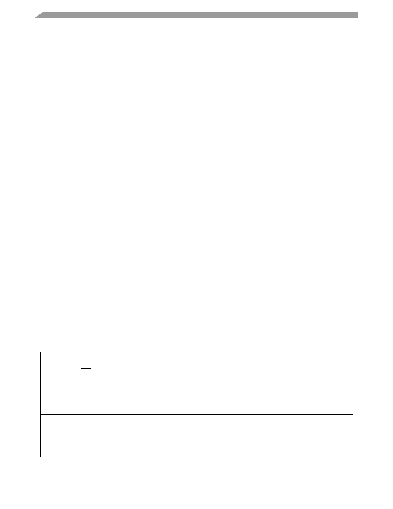
Table 1-1. High True/Low True Signal Conventions
Signal/Symbol
Logic State
Signal State
Voltage
PIN1
True
Asserted
Ground2
PIN
False
Deasserted
VCC3
PIN
True
Asserted
VCC
PIN
False
Deasserted
Ground
Notes: 1.
2.
3.
PIN is a generic term for any pin on the chip.
Ground is an acceptable low voltage level. See the appropriate data sheet for the range of acceptable low
voltage levels (typically a TTL logic low).
VCC is an acceptable high voltage level. See the appropriate data sheet for the range of acceptable high
voltage levels (typically a TTL logic high).
DSP56303 User’s Manual, Rev. 2
1-2
Freescale Semiconductor
Share Link: 