80960CF-40(2002) Просмотр технического описания (PDF) - Intel
Номер в каталоге
Компоненты Описание
производитель
80960CF-40 Datasheet PDF : 70 Pages
| |||
80960-40, -33, -25
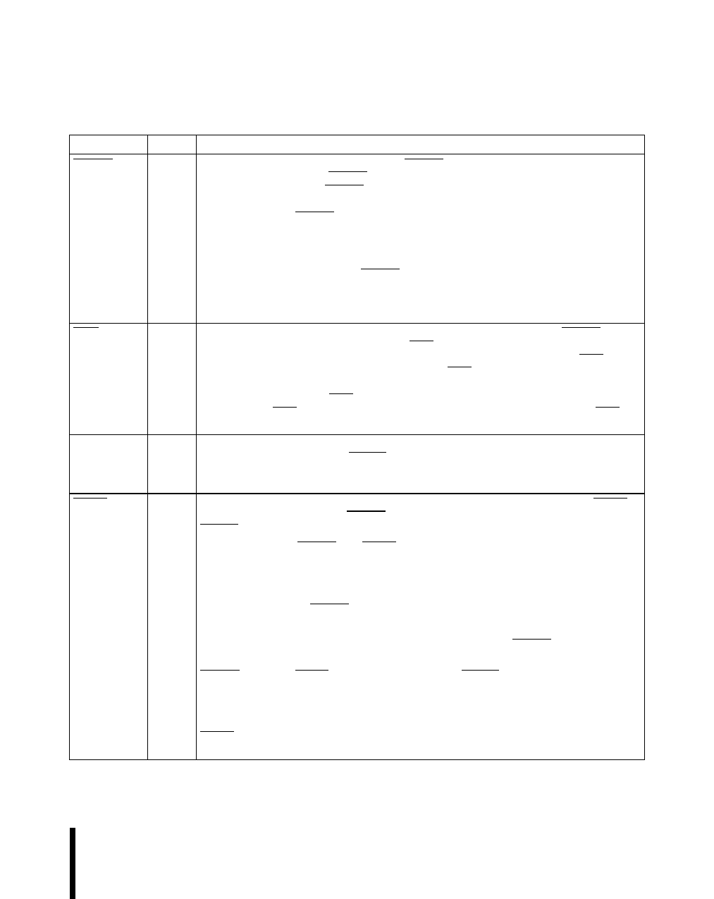
Table 4. 80960CF Pin Description—Processor Control Signals (Sheet 2 of 2)
Name
Type
Description
PCLK2:1
VSS
VCC
VCCPLL
NC
O
S
H(Q)
R(Q)
–
–
–
–
PROCESSOR OUTPUT CLOCKS provide a timing reference for all inputs and
outputs. All input and output timings are specified in relation to PCLK2 and PCLK1.
PCLK2 and PCLK1 are identical signals. Two output pins are provided to allow
flexibility in the system’s allocation of capacitive loading on the clock. PCLK2:1 may
also be connected at the processor to form a single clock signal.
GROUND connections must be connected externally to a VSS board plane.
POWER connections must be connected externally to a VCC board plane.
VCCPLL is a separate VCC supply pin for the phase lock loop used in 1-x clock mode.
Connecting a simple lowpass filter to VCCPLL may help reduce clock jitter (TCP) in
noisy environments. Otherwise, VCCPLL should be connected to VCC.
NO CONNECT pins must not be connected in a system.
Table 5. 80960CF Pin Description—DMA and Interrupt Unit Control Signals
Name
DREQ3:0
DACK3:0
EOP/TC3:0
XINT7:0
NMI
Type
Description
I
A(L)
H(Z)
R(Z)
DMA REQUEST is used to request a DMA transfer. Each of the four signals
requests a transfer on a single channel. DREQ0 requests channel 0, DREQ1
requests channel 1, etc. When two or more channels are requested simultaneously,
the channel with the highest priority is serviced first. Channel priority mode is
programmable.
O DMA ACKNOWLEDGE indicates that a DMA transfer is being executed. Each of
S the four signals acknowledges a transfer for a single channel. DACK0
H(1) acknowledges channel 0, DACK1 acknowledges channel 1, etc. DACK3:0 are
R(1) asserted when the requesting device of a DMA is accessed.
I/O
A(L)
H(Z/Q)
R(Z)
END OF PROCESS/TERMINAL COUNT may be programmed as either an input
(EOP3:0) or output (TC3:0), but not both. Each pin is individually programmable.
When programmed as an input, EOPx causes termination of a current DMA transfer
for the channel that corresponds to the EOPx pin. EOP0 corresponds to channel 0,
EOP1 corresponds to channel 1, etc. When a channel is configured for source and
destination chaining, the EOP pin for that channel causes termination of only the
current buffer transferred and causes the next buffer to be transferred. EOP3:0 are
asynchronous inputs.
When programmed as an output, the channel’s TCx pin indicates that the channel
byte count has reached 0 and a DMA has terminated. TCx is driven with the same
timing as DACKx during the last DMA transfer for a buffer. When the last bus
request is executed as multiple bus accesses, TCx stays asserted for the entire bus
request.
I
A(E/L)
H(Z)
R(Z)
EXTERNAL INTERRUPT PINS cause interrupts to be requested. These pins may
be configured in three modes:
Dedicated Mode: Each pin is a dedicated external interrupt source. Dedicated
inputs may be individually programmed to be level (low) or edge (falling) activated.
Expanded Mode: The eight pins act together as an 8-bit vectored interrupt source.
The interrupt pins in this mode are level activated. Since the interrupt pins are active
low, the vector number requested is the 1’s complement of the positive logic value
place on the port. This eliminates glue logic to interface to combinational priority
encoders which output negative logic.
Mixed Mode: XINT7:5 are dedicated sources and XINT4:0 act as the five most
significant bits of an expanded mode vector. The least significant bits are set to 010
internally.
I
A(E)
H(Z)
R(Z)
NON-MASKABLE INTERRUPT causes a non-maskable interrupt event to occur.
NMI is the highest priority interrupt recognized. NMI is an edge (falling) activated
source.
Datasheet
15
Share Link: 