CXD2951GA-2 Просмотр технического описания (PDF) - Sony Semiconductor
Номер в каталоге
Компоненты Описание
производитель
CXD2951GA-2 Datasheet PDF : 26 Pages
| |||
CXD2951GA-2
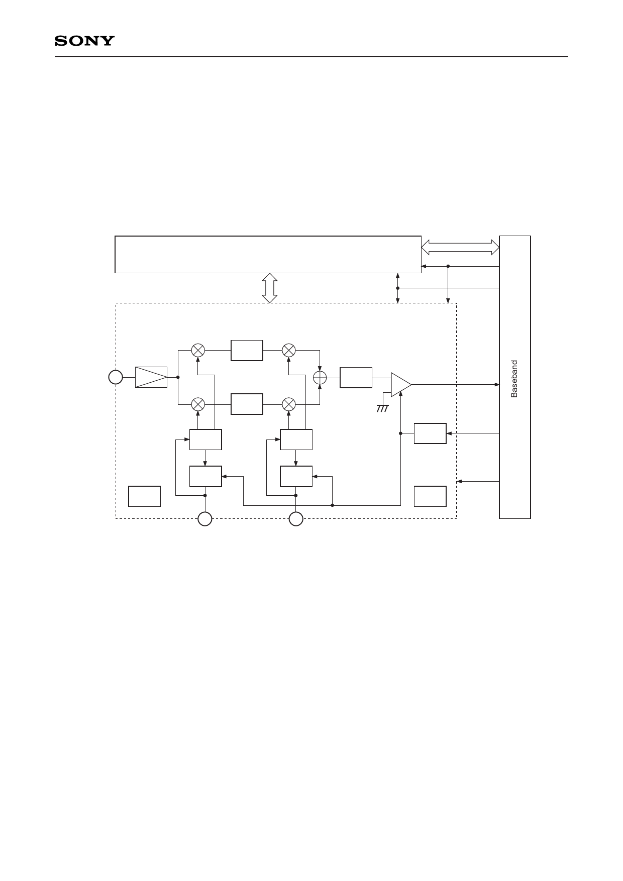
Radio Block Operation
Radio block diagram shows RF section of the chip. The signal flow starts from the RFIN port (Pin 47). The
signal is amplified and mixed down to the first Intermediate Frequency (IF) of 2MHz with cosine and sine wave
quadrature mixers. Out of band images are filtered out and the signal is again mixed down to the 2nd IF of
1MHz with another set of quadrature mixers. The complex signal becomes real with the addition of real and
imaginary components. The image of the 2nd IF mixing is removed with the last Band Pass Filter (BPF). The
real signal is then amplified one last time and transferred to digital baseband processing unit.
RF Digital
Reset
CLK
RFIN
RF Analog
BPF
1st IF (2MHz)
RF Local
(1573MHz)
VCO
BPF
IF Local (3MHz)
VCO
2nd IF (1MHz)
A/D Converter
BPF
Data
BUF
PLLCLK
PLL
PLL
BIAS
TEST
Enable
LPFRF
LPFIF
Radio Block Diagram
To have constant internal frequencies for mixing and other purposes, the supplied TCXO frequency is counted
by a Real Time Clock (RTC), and the internal PLL divider is automatically set to provide correct frequency for
RF mixing and baseband operation.
The loop filters (RF and IF) are externally connected. Use parts that satisfy the required tolerance.
– 20 –
Share Link: 