CM3202-00DE Просмотр технического описания (PDF) - California Micro Devices Corp
Номер в каталоге
Компоненты Описание
производитель
CM3202-00DE Datasheet PDF : 12 Pages
| |||
PRELIMINARY
CM3202
Application Info (cont’d)
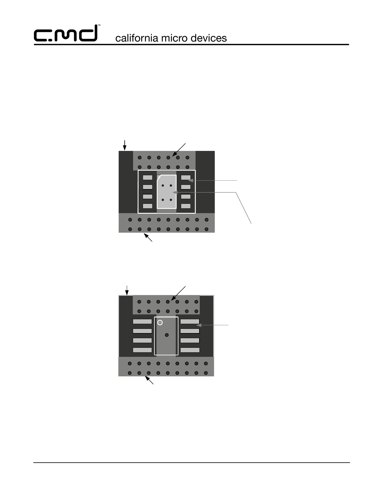
blocking of the solder. The ground and power planes
need to be at least 2 square inches of copper by the
vias. It also helps dissipation if the chip is positioned
away from the edge of the PCB, and not near other
heat-dissipating devices. A good thermal link from the
PCB pad to the rest of the PCB will assure the best
heat transfer from the CM3202-00DE (TDFN-8) to
ambient, θJA, of approximately 42.5 -°C/W, or θJA of
approximately 85 °C/W for the CM3202-00SM (SOIC-
8).
Bottom Layer
Ground Plane
Top View
Top Layer Copper
Connects to Heat Spreader
Pin Solder Mask
Vias (0.3mm Diameter)
(TDFN-8 Package)
Thermal PAD
Solder Mask
Bottom Layer
Ground Plane
Top View
Top Layer Copper
Connects to Heat Spreader
Pin Solder Mask
Vias (0.3mm Diameter)
(SOIC-8 Package)
Note: This drawing is not to scale
Figure 2. Thermal Layout
© 2006 California Micro Devices Corp. All rights reserved.
05/08/06 490 N. McCarthy Blvd., Milpitas, CA 95035-5112 l Tel: 408.263.3214 l Fax: 408.263.7846 l www.cmd.com
10
Share Link: 