CDP1802AC/3 Просмотр технического описания (PDF) - Intersil
Номер в каталоге
Компоненты Описание
производитель
CDP1802AC/3 Datasheet PDF : 27 Pages
| |||
CDP1802AC/3
XTAL
Connection to be used with clock input terminal, for an
external crystal, if the on-chip oscillator is utilized. The
crystal is connected between terminals 1 and 39 (CLOCK
and XTAL) in parallel with a resistance (10M typ).
Frequency trimming capacitors may be required at terminals
1 and 39. For additional information, see Application Note
AN6565.
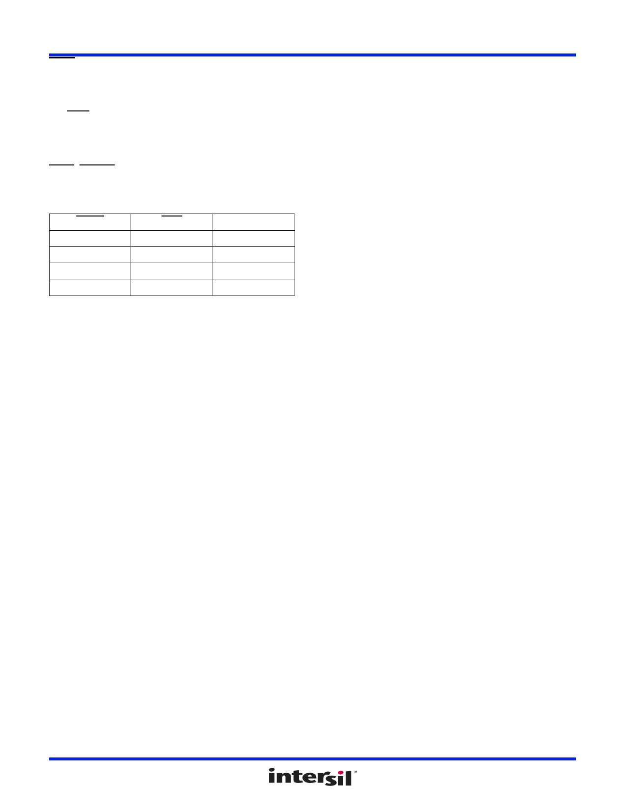
WAIT, CLEAR (2 Control Lines)
Provide four control modes as listed in Table 2:
CLEAR
L
L
H
H
TABLE 2. TRUTH TABLE
WAIT
L
H
L
H
MODE
LOAD
RESET
PAUSE
RUN
VDD, VSS, VCC (Power Levels)
The internal voltage supply VDD is isolated from the
Input/Output voltage supply VCC so that the processor may
operate at maximum speed while interfacing with peripheral
devices operating at lower voltage. VCC must be less than or
equal to VDD. All outputs swing from VSS to VCC. The
recommended input voltage swing is VSS to VCC.
Architecture
The “CPU Block Diagram” is shown on page 3. The principal
feature of this system is a register array (R) consisting of
sixteen 16-bit scratchpad registers. Individual registers in the
array (R) are designated (selected) by a 4-bit binary code
from one of the 4-bit registers labeled N, P and X. The
contents of any register can be directed to any one of the
following three paths:
1. The external memory (multiplexed, higher-order byte
first, on to 8 memory address lines).
2. The D register (either of the two bytes can be gated to D).
3. The increment/decrement circuit where it is increased or
decreased by one and stored back in the selected 16-bit
register.
The three paths, depending on the nature of the instruction,
may operate independently or in various combinations in the
same machine cycle.
With two exceptions, CPU instruction consists of two
8-clock-pulse machine cycles. The first cycle is the fetch
cycle, and the second and third if necessary, are execute
cycles. During the fetch cycle the four bits in the P
designator select one of the 16 registers R(P) as the current
program counter. The selected register R(P) contains the
address of the memory location from which the instruction is
to be fetched. When the instruction is read out from the
memory, the higher order 4 bits of the instruction byte are
FN1441 Rev 3.00
October 17, 2008
loaded into the register and the lower order 4 bits into the N
register. The content of the program counter is automatically
incremented by one so that R(P) is now “pointing” to the next
byte in the memory.
The X designator selects one of the 16 registers R(X) to
“point” to the memory for an operand (or data) in certain ALU
or I/O operations.
The N designator can perform the following five functions
depending on the type of instruction fetched:
1. Designate one of the 16 registers in R to be acted upon
during register operations.
2. Indicate to the I/O devices a command code or device
selection code for peripherals.
3. Indicate the specific operation to be executed during the
ALU instructions, types of test to be performed during the
Branch instruction, or the specific operation required in a
class of miscellaneous instructions (70 - 73 and 78 - 7B).
4. Indicate the value to be loaded into P to designate a new
register to be used as the program counter R(P).
5. Indicate the value to be loaded into X to designate a new
register to be used as data pointer R(X).
The registers in R can be assigned by a programmer in three
different ways: as program counters, as data pointers, or as
scratchpad locations (data registers) to hold two bytes of data.
Program Counters
Any register can be the main program counter; the address
of the selected register is held in the P designator. Other
registers in R can be used as subroutine program counters.
By single instruction the contents of the P register can be
changed to effect a “call” to a subroutine. When interrupts
are being serviced, register R(1) is used as the program
counter for the user's interrupt servicing routine. After reset,
and during a DMA operation, R(0) is used as the program
counter. At all other times the register designated as
program counter is at the discretion of the user.
Data Pointers
The registers in R may be used as data pointers to indicate a
location in memory. The register designated by X (i.e., R(X))
points to memory for the following instructions (see Table 4).
1. ALU operations F1 - F5, F7, 74, 75, 77
2. Output instructions 61 through 67
3. Input instructions 69 through 6F
4. Certain miscellaneous instructions - 70 - 73, 78, 60, F0
The register designated by N (i.e., R(N)) points to memory
for the “load D from memory” instructions 0N and 4N and the
“Store D” instruction 5N. The register designated by P (i.e.,
the program counter) is used as the data pointer for ALU
instructions F8 - FD, FF, 7C, 7D, 7F. During these instruction
executions, the operation is referred to as “data immediate”.
Another important use of R as a data pointer supports the
built-in Direct-Memory-Access (DMA) function. When a
Page 16 of 27
Share Link: 