BD234G(2013) Просмотр технического описания (PDF) - ON Semiconductor
Номер в каталоге
Компоненты Описание
производитель
BD234G Datasheet PDF : 5 Pages
| |||
BD237G (NPN), BD234G, BD238G (PNP)
ÎÎÎÎELEÎÎCTÎÎRICÎÎAL ÎÎCHAÎÎRAÎÎCTEÎÎRISÎÎTICÎÎS (TÎÎC=ÎÎ25_CÎÎunÎÎlessÎÎotheÎÎrwisÎÎe noÎÎted)ÎÎÎÎÎÎÎÎÎÎÎÎÎÎÎÎÎÎÎÎÎÎÎÎÎÎÎÎ
Characteristic
Symbol
Min
Max
Unit
Collector−Emitter Sustaining Voltage (Note 1)
(IC = 0.1 Adc, IB = 0)
BD237G, BD238G
BD234G
V(BR)CEO
80
45
Vdc
−
−
Collector Cutoff Current
(VCB = 100 Vdc, IE = 0)
BD237G, BD238G
(VCB = 60 Vdc, IE = 0)
BD234G
ICBO
−
−
mAdc
0.1
0.1
Emitter Cutoff Current
(VBE = 5.0 Vdc, IC = 0)
IEBO
−
mAdc
1.0
DC Current Gain
(IC = 0.15 A, VCE = 2.0 V)
(IC = 1.0 A, VCE = 2.0 V)
−
hFE1
40
−
hFE2
25
−
Collector−Emitter Saturation Voltage (Note 1)
(IC = 1.0 Adc, IB = 0.1 Adc)
VCE(sat)
−
Vdc
0.6
Base−Emitter On Voltage (Note 1)
(IC = 1.0 Adc, VCE = 2.0 Vdc)
VBE(on)
−
Vdc
1.3
Current−Gain − Bandwidth Product
(IC = 250 mAdc, VCE = 10 Vdc, f = 1.0 MHz)
fT
MHz
3.0
−
Product parametric performance is indicated in the Electrical Characteristics for the listed test conditions, unless otherwise noted. Product
performance may not be indicated by the Electrical Characteristics if operated under different conditions.
1. Pulse Test: Pulse Width ≤ 300 ms, Duty Cycle ≤ 2.0%.
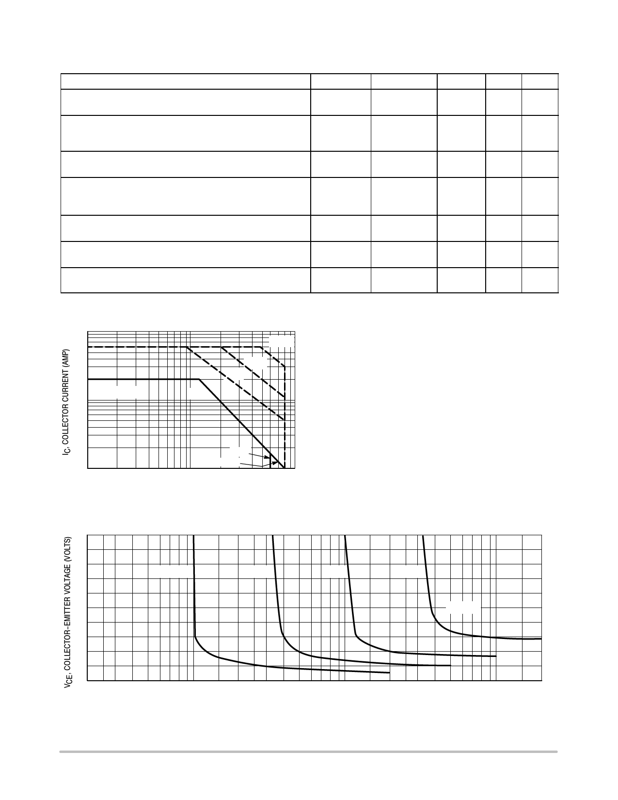
10
3
TJ = 150°C
1
100 ms
The Safe Operating Area Curves indicate IC−VCE limits
below which the device will not enter secondary breakdown.
1 ms
5 ms
dc
Collector load lines for specific circuits must fall within the
applicable Safe Area to avoid causing a catastrophic failure.
To insure operation below the maximum TJ,
power−temperature derating must be observed for both
steady state and pulse power conditions.
0.3
0.1
1
3
BD236
BD237
10
30
100
VCE, COLLECTOR-EMITTER VOLTAGE (VOLTS)
Figure 1. Active Region Safe Operating Area
http://onsemi.com
2
Share Link: 