W91460N Просмотр технического описания (PDF) - Winbond
Номер в каталоге
Компоненты Описание
производитель
W91460N Datasheet PDF : 15 Pages
| |||
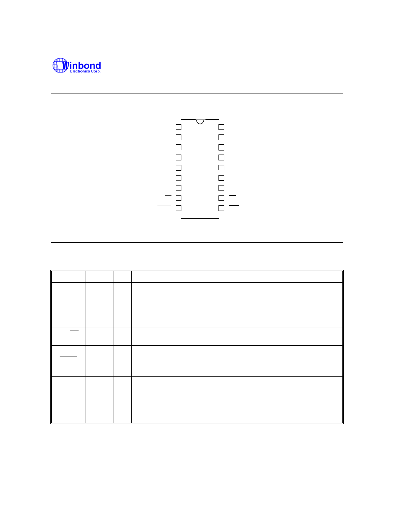
PIN CONFIGURATION
W91460N SERIES
C1 1
C2 2
C3 3
C4 4
C5 5
VSS
6
XT 7
XT 8
T/P MUTE 9
18 R4
17 R3
16 R2
15 R1
14
VDD
13 MODE
12 DTMF
11 DP
10 HKS
PIN DESCRIPTION
SYMBOL PIN I/O
FUNCTION
Column-
Row
Inputs
1−5
&
15−18
I The keyboard inputs may be used with either a standard 5 × 5
keyboard or an inexpensive single contact (Form A) keyboard.
Electronic input from a µC can also be used.
A valid key-in is defined as a single row being connected to a single
column.
XT, XT
7, 8 I, O A built-in inverter provides oscillation with an inexpensive 3.579545
MHz crystal or ceramic resonator.
T/P
MUTE
9
O The T/P MUTE is a conventional CMOS N-channel open drain output.
The output transistor is switched on during dialing sequence and flash
break time. Otherwise, it is switched off.
MODE
13
I Pulling mode pin to VSS places the dialer in tone mode.
Pulling mode pin to VDD places the dialer in pulse mode with M/B ratio
40:60 (10 ppS for W91462N and 20 ppS for W91466N).
Floating mode pin places the dialer in pulse mode with M/B ratio
33.3:66.7 (10 ppS for W91462N and 20 ppS for W91466N).
-2-
Share Link: 