AT90S8515 Просмотр технического описания (PDF) - Atmel Corporation
Номер в каталоге
Компоненты Описание
производитель
AT90S8515 Datasheet PDF : 112 Pages
| |||
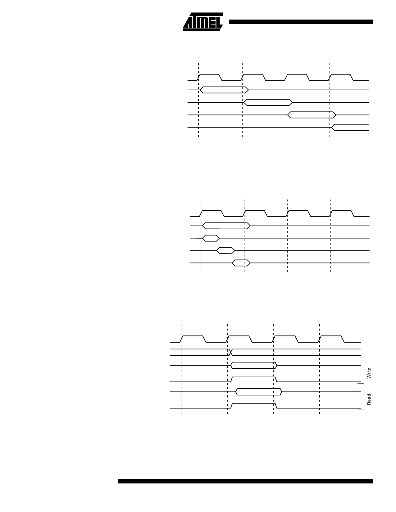
Figure 20. The Parallel Instruction Fetches and Instruction Executions
T1
T2
T3
T4
System Clock Ø
1st Instruction Fetch
1st Instruction Execute
2nd Instruction Fetch
2nd Instruction Execute
3rd Instruction Fetch
3rd Instruction Execute
4th Instruction Fetch
Figure 21 shows the internal timing concept for the register file. In a single clock cycle
an ALU operation using two register operands is executed and the result is stored back
to the destination register.
Figure 21. Single Cycle ALU Operation
T1
T2
T3
T4
System Clock Ø
Total Execution Time
Register Operands Fetch
ALU Operation Execute
Result Write Back
The internal data SRAM access is performed in two System Clock cycles as described
in Figure 22.
Figure 22. On-chip Data SRAM Access Cycles
T1
T2
T3
T4
System Clock Ø
Address
Data
WR
Data
RD
Prev. Address
Address
See “Interface to External SRAM” on page 60 for a description of the access to the
external SRAM.
18 AT90S8515
0841G–09/01
Share Link: 