AP2218T-3.3 Просмотр технического описания (PDF) - BCD Semiconductor
Номер в каталоге
Компоненты Описание
производитель
AP2218T-3.3 Datasheet PDF : 13 Pages
| |||
1A LOW DROPOUT LINEAR REGULATOR
1A LOW DROPOUT LINEAR REGULATOR
Preliminary Datasheet
AP2218
AP2218
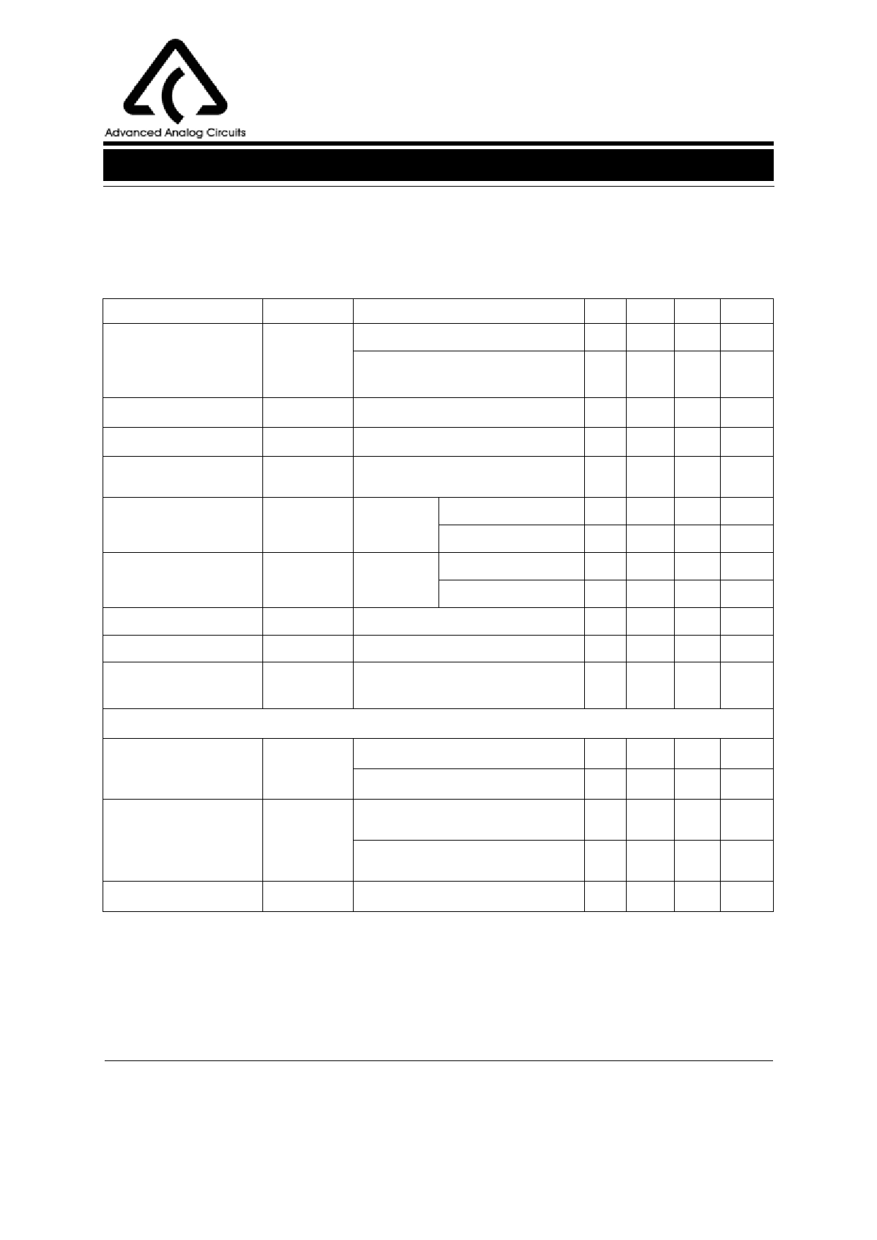
Electrical Characteristics
AP2218-3.3V Electrical Characteristics
Operating Conditions: VIN=4.3V, CIN=10µF, COUT=10µF, TJ=25oC, unless otherwise specified. The Boldface
applies over -40oC≤TJ≤125oC. (P≤maximum power dissipation.)
Parameter
Symbol
Condition
Min Typ Max Unit
Output Voltage
VOUT
IOUT=10mA
10mA≤IOUT≤1A, 4.3V≤VIN≤6.3V
(Note 2)
3.27 3.3 3.33 V
3.23
3.37 V
Line Regulation
Load Regulation
Output Voltage
Temperature Coefficient
Dropout Voltage (Note 3)
Ground Current
Current Limit
Minimum Load Current
Output Noise Voltage (rms)
Enable Input
VRLINE
VRLOAD
∆VOUT/∆T
IOUT=10mA, 4.3V≤VIN≤8V
VIN=4.3V, 10mA≤IOUT≤1A
IOUT=10mA
VDROP
IGND
ILIMIT
ILOAD(MIN)
∆VOUT=1% IOUT=100mA
IOUT=1A
VIN=4.3V
IOUT=750mA
IOUT=1A
VOUT=0V (Note 4)
10Hz to 100KHz, IOUT=100mA,
COUT=10µF
3.3 33 mV
6.6 50 mV
66 330 µV/oC
70 200 mV
300 550 mV
6
15 mA
10
mA
1.5 2.2
A
1
5
mA
400
µV
Enable Input Voltage
VEN
Logic low (off)
Logic high (on)
0.8
V
2.25
V
Enable Input Current
IIN
VEN=2.25V
VEN=0.8V
Shutdown Output Current IOUT(SHDN) (Note 5)
1
15
30
µA
75
2
µA
4
10
20
µA
Note 2: For the details of VIN range, please refer to (VIN-VOUT)*ILOAD≤maximum power dissipation (Figure 4).
Note 3: Dropout voltage is defined as the input-to-output differential when the output voltage drops to 99% of its nominal value
which is measured at VOUT+1V applied to VIN.
Note 4: VIN=VOUT(NOMINAL)+1V.
Note 5: VEN ≤0.8V, VIN≤8V, VOUT=0V.
Aug. 2005 Rev. 1. 0
BCD Semiconductor Manufacturing Limited
5
Share Link: 