ADXL346 –ü—Ä–æ—Å–º–æ—Ç—Ä —Ç–µ—Ö–Ω–∏—á–µ—Å–∫–æ–≥–æ –æ–ø–∏—Å–∞–Ω–∏—è (PDF) - Analog Devices
–ù–æ–º–µ—Ä –≤ –∫–∞—Ç–∞–ª–æ–≥–µ
–ö–æ–º–ø–æ–Ω–µ–Ω—Ç—ã –û–ø–∏—Å–∞–Ω–∏–µ
–ø—Ä–æ–∏–∑–≤–æ–¥–∏—Ç–µ–ª—å
ADXL346 Datasheet PDF : 40 Pages
| |||
ADXL346
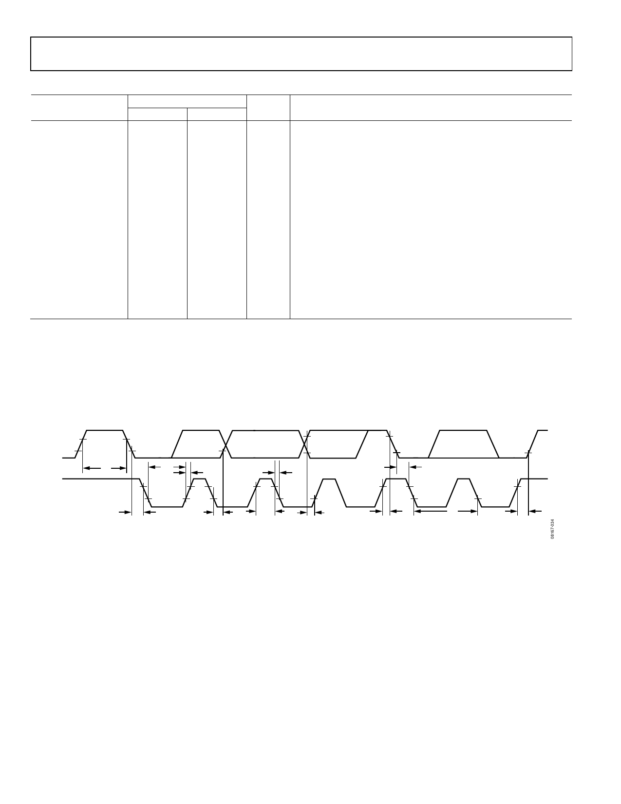
Table 12. I2C Timing (TA = 25°C, VS = 2.6 V, VDD I/O = 1.8 V)
Limit1, 2
Parameter
Min
Max
Unit
fSCL
400
kHz
t1
2.5
μs
t2
0.6
μs
t3
1.3
μs
t4
0.6
μs
t5
t63, 4, 5, 6
100
ns
0
0.9
μs
t7
0.6
μs
t8
0.6
μs
t9
1.3
μs
t10
300
ns
0
ns
t11
250
ns
300
ns
20 + 0.1 CB7
ns
CB7
400
pF
Description
SCL clock frequency
SCL cycle time
tHIGH, SCL high time
tLOW, SCL low time
tHD, STA, start/repeated start condition hold time
tSU, DAT, data setup time
tHD, DAT, data hold time
tSU, STA, setup time for repeated start
tSU, STO, stop condition setup time
tBUF, bus-free time between a stop condition and a start condition
tR, rise time of both SCL and SDA when receiving
tR, rise time of both SCL and SDA when receiving or transmitting
tF, fall time of SDA when receiving
tF, fall time of both SCL and SDA when transmitting
tF, fall time of both SCL and SDA when transmitting or receiving
Capacitive load for each bus line
1 Limits are based on characterization results, with fSCL = 400 kHz and a 3 mA sink current; not production tested.
2 All values referred to the VIH and the VIL levels given in Table 11.
3 t6 is the data hold time that is measured from the falling edge of SCL. It applies to data in transmission and acknowledge.
4 A transmitting device must internally provide an output hold time of at least 300 ns for the SDA signal (with respect to VIH,min of the SCL signal) to bridge the undefined region of
the falling edge of SCL.
5 The maximum t6 value must be met only if the device does not stretch the low period (t3) of the SCL signal.
6 The maximum value for t6 is a function of the clock low time (t3), the clock rise time (t10), and the minimum data setup time (t5(min)). This value is calculated as t6(max) = t3 ‚àí t10 ‚àí t5(min).
7 CB is the total capacitance of one bus line in picofarads.
SDA
t9
t3
t10
t11
t4
SCL
t4
START
CONDITION
t6
t2
t5
t7
t1
REPEATED
START
CONDITION
Figure 41. I2C Timing Diagram
t8
STOP
CONDITION
Rev. 0 | Page 18 of 40
Share Link: 