ADP3810AR-126 Просмотр технического описания (PDF) - Analog Devices
Номер в каталоге
Компоненты Описание
производитель
ADP3810AR-126 Datasheet PDF : 16 Pages
| |||
ADP3810/ADP3811
GM4
CF1
POWER
1nF
STAGE
∆VC
R
2R
VX
AV2 = 0.33V/V
COMP
RF
CF
3.3kΩ 1nF
VFB
+5V
VOLTAGE ERROR
AMPLIFIER
VCTRL
1.0V
OUT
OPTO COUPLER
ITXOC = 0.36mA/mA
R4
1.2kΩ
RCS
0.25Ω
CF2
220µF
R3
20kΩ
RC2
300Ω
CC2
0.2µF
VBAT
R1
80.6kΩ
R2
20kΩ
BATTERY
80kΩ
VCS
2.0V VSENSE
GM3
6mA/V
GM1
8.3mA/V
R6
200Ω
ADP3810/
ADP3811
R5
400kΩ
COMP
RC1
CC1
GM 2
2.1mA/V
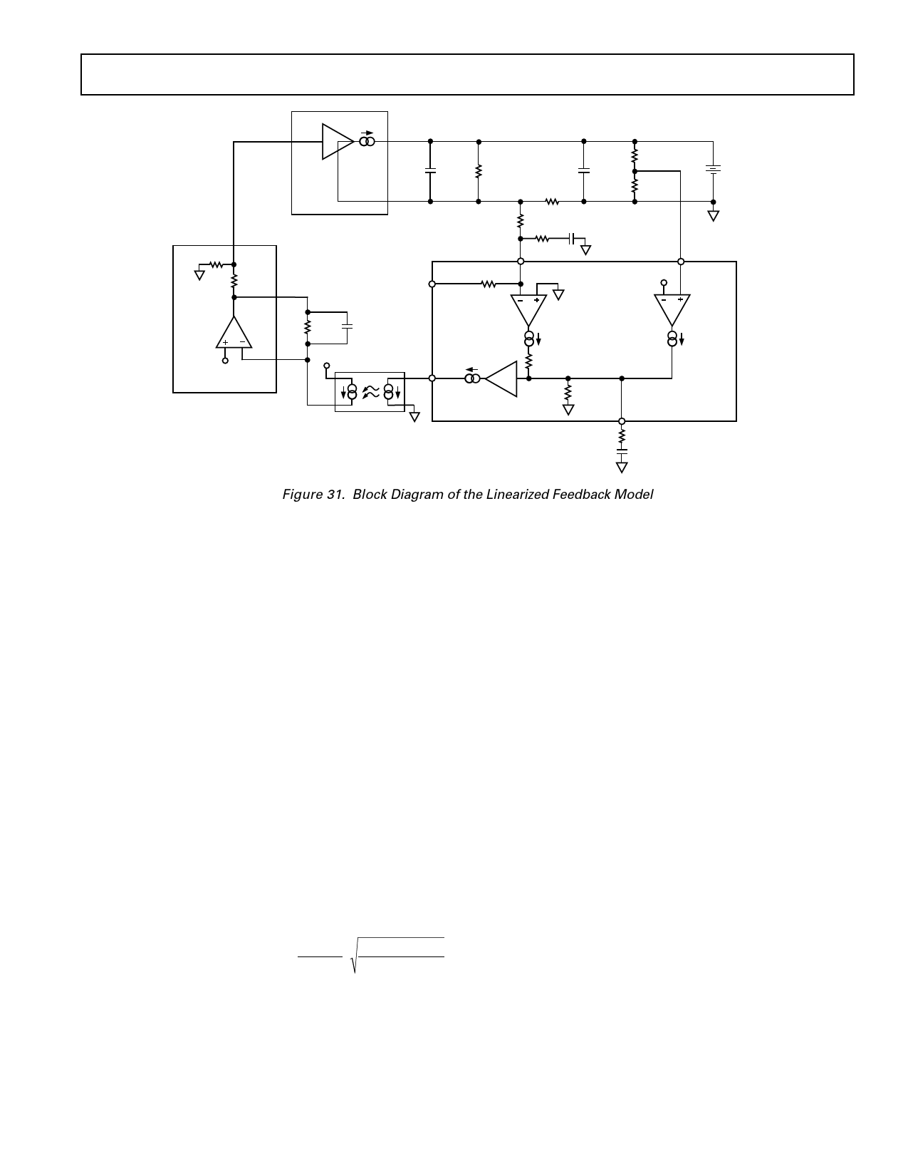
Figure 31. Block Diagram of the Linearized Feedback Model
amplifiers are represented by voltage controlled current sources,
the optocoupler by a current controlled current source, and the
error amplifier by a voltage controlled voltage source.
Design Criteria
Charging a 6 cell NiCad battery.
Max Battery Stack Voltage: VOMAX = 6 × 1.67 V = 10 V
Max Charge Current:
IOMAX = 1 A
RS Fixed Value:
RS = 20 kΩ
Pick a value for R1:
R1 = 80.6 kΩ
Calculated Current Sense
Resistor:
RCS = 0.25 Ω
Calculated Voltage Sense
Divider:
R2 = 20 kΩ
Output Filter Cap:
2nd Filter Cap:
CF1 = 1 mF (ESR = 0.1 Ω)
CF2 = 200 µF (ESR = 0.2 Ω)
Gain of Each Block
ADP3810/ADP3811
VCS Input:
ADP3810/ADP3811
VSENSE Input:
ADP3810/ADP3811
Output Buffer:
Optocoupler:
Voltage Error Amplifier:
GM1 = 8.3 mA/V
GM2 = 2.1 mA/V
GM3 = 6 mA/V
ITXoc = 0.36 mA/mA
AV2 = ∆VC/VX = 0.333
Power Stage (General):
GM4
=
∆IOMAX
∆V C
V OMAX
IOMAX × RLOAD
Power Stage
(Voltage Loop):
GM4 = 0.091 A/V
Power Stage
(Current Loop):
GM4 = 1.0 A/V
The gains for the ADP3810/ADP3811 GM amplifiers are based
on typical measurements of the IC’s open-loop gain, and they
are expressed in units of milliamps per volt. The dc voltage gain
of these stages is the value of GM times the load resistance. At the
COMP pin, the internal load resistance, R5, is typically 400 kΩ.
The optocoupler gain is the typical value taken from the
MOC8103 data sheet. The voltage error amplifier gain is due
to the resistor divider internal to the 3845 only. VX is the out-
put of the internal amplifier, as labeled in Figure 31. The actual
op amp is assumed to have sufficient open-loop gain and band-
width compared to the system bandwidth; as a result, it can be
considered an ideal transimpedance amplifier. The pole created
by the 1 nF capacitor in parallel with RF is high enough in fre-
quency to not affect the compensation.
The power stage gain equation is linearized based on primary
side current mode control with the flyback transformer operat-
ing with discontinuous inductor current. ∆IOMAX is the maxi-
mum change in output current, which is equal to IOMAX–IOMIN.
Since the minimum current is 0.0 A, ∆IOMAX = IOMAX = 1 A. The
maximum change in control voltage is set by internal circuitry
within the 3845 to ∆VC = 1 V. The load resistor, RLOAD, is dif-
ferent for the voltage and current loop cases. For the voltage
loop without the battery, the effective load is R4, but for the
current loop, the effective load is RCS. In the current loop, the
voltage limit has not been reached, so the maximum output
voltage is equal to the maximum output current times the load
resistor. Thus, the entire expression under the square root re-
duces to 1.0. Substituting these values into the general equation
for the power stage yields the specific gain values shown for
GM4.
When calculating the loop gain for the voltage loop and the cur-
rent loop, there are two main differences. First, GM2 applies
only to the voltage loop, and GM1 applies only to the current
loop. Use the appropriate GM input stage for the particular
loop calculations. Second, there are three battery conditions to
consider. For the current loop, the battery is present and un-
charged. Thus, the battery is modeled as a very large capaci-
tance (greater than 1 Farad). For the voltage loop, the battery is
REV. 0
–13–
Share Link: 