ADD5203ACPZ-RL Просмотр технического описания (PDF) - Analog Devices
Номер в каталоге
Компоненты Описание
производитель
ADD5203ACPZ-RL
Analog Devices

ADD5203ACPZ-RL Datasheet PDF : 24 Pages
| |||
ADD5203
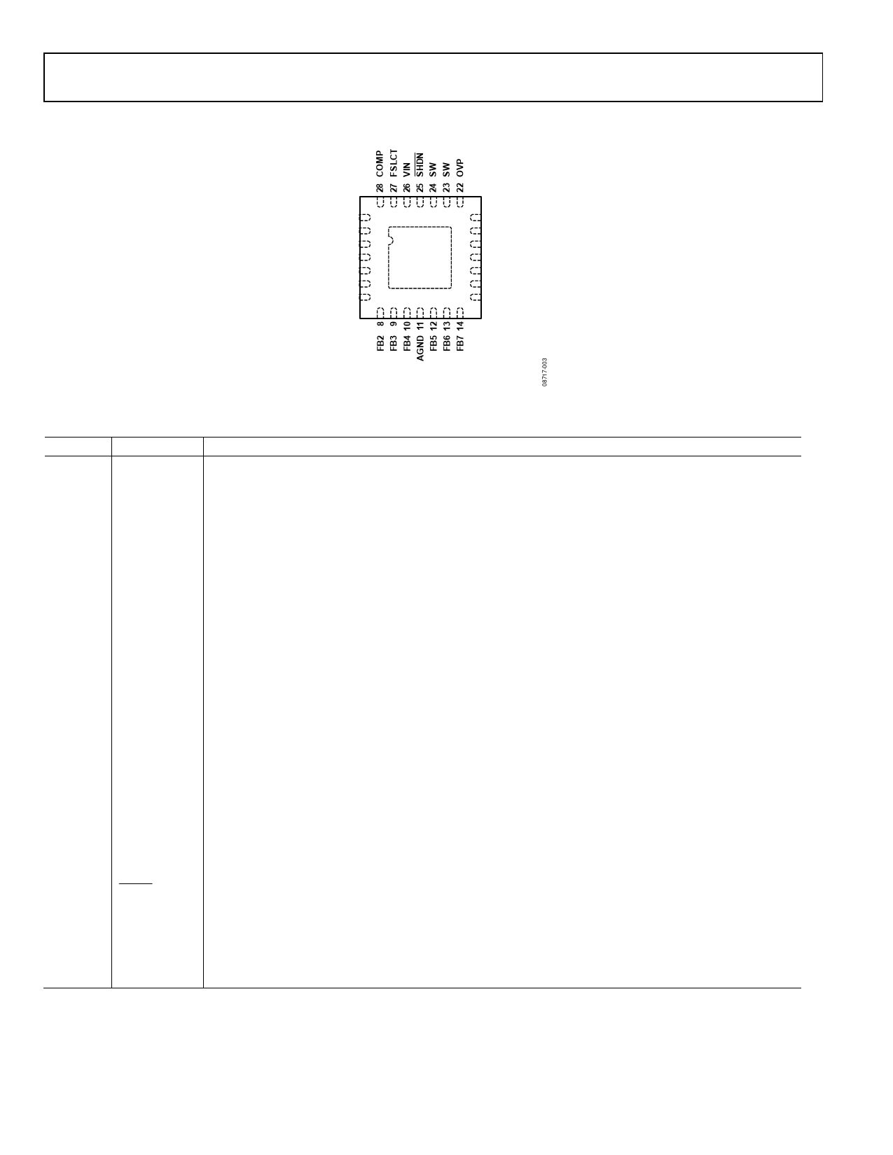
PIN CONFIGURATION AND FUNCTION DESCRIPTIONS
PWMI 1
SEL1 2
SEL2 3
VDDIO 4
SDA 5
SCL 6
FB1 7
ADD5203
TOP VIEW
(Not to Scale)
21 PGND
20 PGND
19 C_FPWM
18 R_FPWM
17 ISET
16 NC
15 FB8
NOTES
1. NC = NO CONNECT.
2. CONNECT THE EXPOSED PADDLE TO GND.
Figure 3. Pin Configuration
Table 7. Pin Function Descriptions
Pin No. Mnemonic Description
1
PWMI
PWM Signal Input.
2
SEL1
Dimming Mode Selection 1.
3
SEL2
Dimming Mode Selection 2.
4
VDDIO
Internal Linear Regulator Output. This regulator provides power to the ADD5203.
5
SDA
Serial Data Input/Output.
6
SCL
Serial Clock Input.
7
FB1
Regulated Current Sink. Connect the bottom cathode of the LED string to this pin.
8
FB2
Regulated Current Sink. Connect the bottom cathode of the LED string to this pin.
9
FB3
Regulated Current Sink. Connect the bottom cathode of the LED string to this pin.
10
FB4
Regulated Current Sink. Connect the bottom cathode of the LED string to this pin.
11
AGND
Analog Ground.
12
FB5
Regulated Current Sink. Connect the bottom cathode of the LED string to this pin. If unused, connect to GND.
13
FB6
Regulated Current Sink. Connect the bottom cathode of the LED string to this pin. If unused, connect to GND.
14
FB7
Regulated Current Sink. Connect the bottom cathode of the LED string to this pin. If unused, connect to GND.
15
FB8
Regulated Current Sink. Connect the bottom cathode of the LED string to this pin. If unused, connect to GND.
16
NC
No Connection.
17
ISET
Full-Scale LED Current Set. A resistor from this pin to ground sets the LED current up to 30 mA.
18
R_FPWM
Dimming frequency adjustment pin with an external resistor.
19
C_FPWM
Dimming frequency adjustment pin with an external capacitor.
20
PGND
Power Ground.
21
PGND
Power Ground.
22
OVP
Overvoltage Protection.
23
SW
Drain Connection of the Internal Power FET.
24
SW
Drain Connection of the Internal Power FET.
25
SHDN
Shutdown Control for PWM Input Operation Mode. Active low.
26
VIN
Supply Input. Must be locally bypassed with a capacitor to ground.
27
FSLCT
Frequency Select. A resistor from this pin to ground sets the boost switching frequency from 350 kHz to 1 MHz.
28
COMP
Compensation for Boost Converter. A capacitor and a resistor are connected in series between ground and
this pin for stable operation and an optional capacitor can be connected from this pin to ground.
EP
Exposed Paddle. Connect the exposed paddle to ground.
Rev. 0 | Page 8 of 24
Share Link: