AD7818ARMZ-REEL7 Просмотр технического описания (PDF) - Analog Devices
Номер в каталоге
Компоненты Описание
производитель
AD7818ARMZ-REEL7 Datasheet PDF : 20 Pages
| |||

AD7817/AD7818
Read Operation
Figure 21 shows the timing diagram for a serial read from the
AD7817. CS is brought low to enable the serial interface, and
RD/WR is set logic high to indicate that the data transfer is a
serial read from the AD7817. The rising edge of RD/WR clocks
out the first data bit (DB9), subsequent bits are clocked out on
the falling edge of SCLK (except for the first falling SCLK edge)
and are valid on the rising edge. During a read operation, 10 bits of
data are transferred. However, a choice is available to only clock
eight bits if the full 10 bits of the conversion result are not required.
The serial data can be accessed in a number of bytes if 10 bits of
data are being read. However, RD/WR must remain high for the
duration of the data transfer operation. Before starting a new data
read operation, the RD/WR signal must be brought low and high
again. At the end of the read operation, the DOUT line enters a high
impedance state on the rising edge of the CS, or the falling edge of
RD/WR, whichever occurs first. The readback process is a
destructive process, in that once data is read back, it is erased. A
conversion must be done again; otherwise, no data is read back.
Write Operation
Figure 21 also shows the control byte write operation to the
AD7817. The RD/WR input goes low to indicate to the part that
a serial write is about to occur. The AD7817 control byte is loaded
on the rising edge of the first eight clock cycles of the serial clock
with data on all subsequent clock cycles being ignored. To carry
out a second successive write operation, the RD/WR signal must be
brought high and low again.
Simplifying the Serial Interface
To minimize the number of interconnect lines to the AD7817,
connect the CS line to DGND. This is possible if the AD7817 is
not sharing the serial bus with another device. It is also possible to
tie the DIN and DOUT lines together. This arrangement is compatible
with the 8051 microcontroller. The 68HC11, 68HC05, and
PIC16Cxx can be configured to operate with a single serial data
line. In this way, the number of lines required to operate the serial
interface can be reduced to three, that is, RD/WR, SCLK, and
DIN/DOUT (see Figure 8).
Data Sheet
AD7818 SERIAL INTERFACE MODE
The serial interface on the AD7818 is a 3-wire interface that has
read and write capabilities. Data is read from the output register
and the control byte is written to the AD7818 via the DIN/DOUT
line. The AD7818 operates in slave mode and requires an externally
applied serial clock to the SCLK input to access data from the
data register or write to the control byte. The RD/WR line is
used to determine whether data is being written to or read from
the AD7818. When data is being written to the AD7818, the
RD/WR line is set logic low, and when data is being read from
the AD7818 the line is set logic high (see Figure 22). The serial
interface on AD7818 is designed to allow the AD7818 to interface
with systems that provide a serial clock that is synchronized to
the serial data, such as the 80C51, 87C51, 68HC11, 68HC05,
and PIC16Cxx microcontrollers.
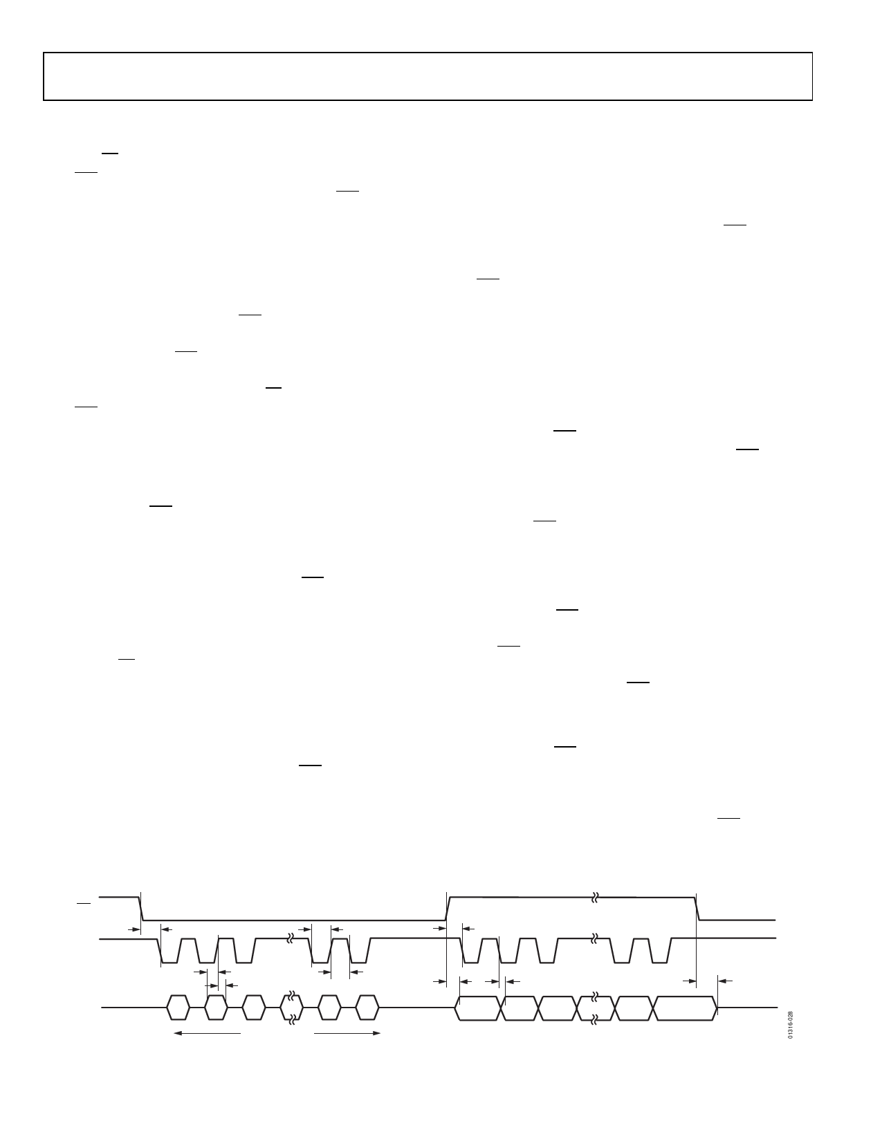
Read Operation
Figure 22 shows the timing diagram for a serial read from the
AD7818. The RD/WR is set logic high to indicate that the data
transfer is a serial read from the devices. When RD/WR is logic
high, the DIN/DOUT pin becomes a logic output, and the first data
bit (DB9) appears on the pin. Subsequent bits are clocked out on
the falling edge of SCLK, starting with the second SCLK falling
edge after RD/WR goes high, and are valid on the rising edge of
SCLK. Ten bits of data are transferred during a read operation.
However, a choice is available to only clock eight bits if the full
10 bits of the conversion result are not required. The serial data
can be accessed in a number of bytes if 10 bits of data are being
read. However, RD/WR must remain high for the duration of the
data transfer operation. To carry out a successive read operation,
the RD/WR pin must be brought logic low and high again. At
the end of the read operation, the DIN/DOUT pin becomes a logic
input on the falling edge of RD/WR.
Write Operation
A control byte write operation to the AD7818 is also shown in
Figure 22. The RD/WR input goes low to indicate to the part that a
serial write is about to occur. The AD7818 control bytes are
loaded on the rising edge of the first eight clock cycles of the serial
clock with data on all subsequent clock cycles being ignored. To
carry out a successive write to the AD7818 the RD/WR pin must
be brought logic high and low again.
RD/WR
SCLK
DIN/OUT
t5
1
2
3
t6
t7
DB7 DB6 DB5
t8
7
8
t9
DB1 DB0
t11
1
2
3
t12
t13
DB9
DB8 DB7
CONTROL BYTE
Figure 22. AD7818 Serial Interface Timing Diagram
Rev. D | Page 18 of 20
9
10
DB1
t14a
DB0