AD7818ARZ Просмотр технического описания (PDF) - Analog Devices
Номер в каталоге
Компоненты Описание
производитель
AD7818ARZ Datasheet PDF : 20 Pages
| |||
AD7817/AD7818
CIRCUIT INFORMATION
The AD7817/AD7818 are single- and four-channel, 9 µs
conversion time, 10-bit ADCs with an on-chip temperature
sensor, reference, and serial interface logic functions on a single
chip. The ADC section consists of a conventional, successive
approximation converter based around a capacitor DAC. The
AD7817/AD7818 are capable of running on a 2.7 V to 5.5 V power
supply, and they accept an analog input range of 0 V to VREF.
The on-chip temperature sensor allows an accurate measurement
of the ambient device temperature to be made. The working
measurement range of the temperature sensor is −55°C to +125°C.
The AD7817/AD7818 require a 2.5 V reference, which can be
provided from their internal reference or from an external
reference source. The on-chip reference is selected by connecting
the REFIN pin to analog ground.
CONVERTER DETAILS
Conversion is initiated by pulsing the CONVST input. The
conversion clock for the part is internally generated; therefore,
an external clock is not required, except when reading from and
writing to the serial port. The on-chip, track-and-hold goes from
track mode to hold mode, and the conversion sequence is started
on the falling edge of the CONVST signal. At this point, the BUSY
signal goes high and low again 9 µs or 27 µs later (depending on
whether an analog input or the temperature sensor is selected)
to indicate the end of the conversion process. A microcontroller
can use this signal to determine when the result of the conversion
should be read. The track-and-hold acquisition time of the
AD7817/AD7818 is 400 ns.
A temperature measurement is made by selecting the Channel 0
of the on-chip mux and carrying out a conversion on this channel.
A conversion on Channel 0 takes 27 µs to complete. Temperature
measurement is explained in the Temperature Measurement
section.
The on-chip reference is not available, however, REFIN can be
overdriven by an external reference source (2.5 V only). The effect
of reference tolerances on temperature measurements is discussed
in the Temperature Measurement Error Due to Reference Error
section.
Tie all unused analog inputs to a voltage within the nominal
analog input range to avoid noise pickup. For minimum power
consumption, tie the unused analog inputs to AGND.
Data Sheet
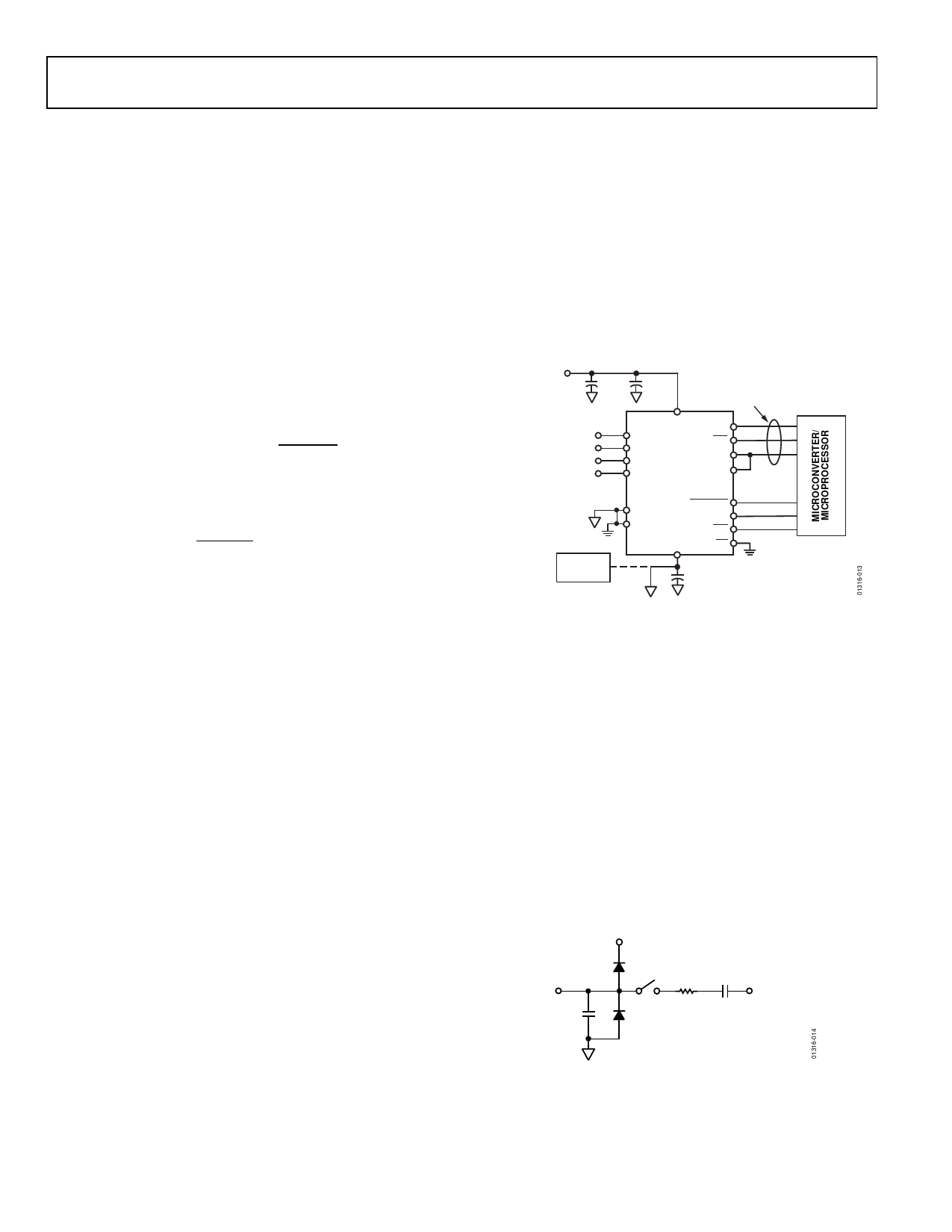
TYPICAL CONNECTION DIAGRAM
Figure 8 shows a typical connection diagram for the AD7817.
The AGND and DGND are connected together at the device for
good noise suppression. The BUSY line is used to interrupt the
microcontroller at the end of the conversion process, and the
serial interface is implemented using three wires (see the AD7817
Serial Interface section for more details). An external 2.5 V
reference can be connected at the REFIN pin. If an external reference
is used, connect a 10 µF capacitor between REFIN and AGND.
For applications where power consumption is a concern, use the
automatic power-down at the end of a conversion to improve
power performance. See the Power vs. Throughput section.
SUPPLY
2.7V TO 5.5V
10µF
0.1µF
3-WIRE
SERIAL
INTERFACE
0V TO 2.5V
INPUT
VDD SCLK
AIN1
RD/WR
AIN2
DOUT
AIN3
AIN4 AD7817
DIN
OPTIONAL
EXTERNAL
REFERENCE
AD780/
REF-192
AGND
DGND
CONVST
BUSY
OTI
REFIN
CS
10µF
EXTERNAL
REFERENCE
Figure 8. Typical Connection Diagram
ANALOG INPUTS
Analog Input
Figure 9 shows an equivalent circuit of the analog input structure of
the AD7817/AD7818. The two diodes, D1 and D2, provide ESD
protection for the analog inputs. Take care to ensure that the
analog input signal never exceeds the supply rails by more than
200 mV. This causes these diodes to become forward-biased
and start conducting current into the substrate. The maximum
current these diodes can conduct without causing irreversible
damage to the part is 20 mA. The C2 capacitor in Figure 9 is
typically about 4 pF and can mostly be attributed to pin
capacitance. The R1 resistor is a lumped component made up
of the on resistance of a multiplexer and a switch. This resistor
is typically about 1 kΩ. The C1 capacitor is the ADC sampling
capacitor and has a capacitance of 3 pF.
VDD
AIN
C2
4pF
D1
C1
R1
3pF
1kΩ
VBALANCE
D2
CONVERT PHASE—SWITCH OPEN
TRACK PHASE—SWITCH CLOSED
Figure 9. Equivalent Analog Input Circuit
Rev. D | Page 12 of 20
Share Link: 