ACST2 Просмотр технического описания (PDF) - STMicroelectronics
Номер в каталоге
Компоненты Описание
производитель
ACST2 Datasheet PDF : 11 Pages
| |||
Characteristics
1
Characteristics
ACST2 Series
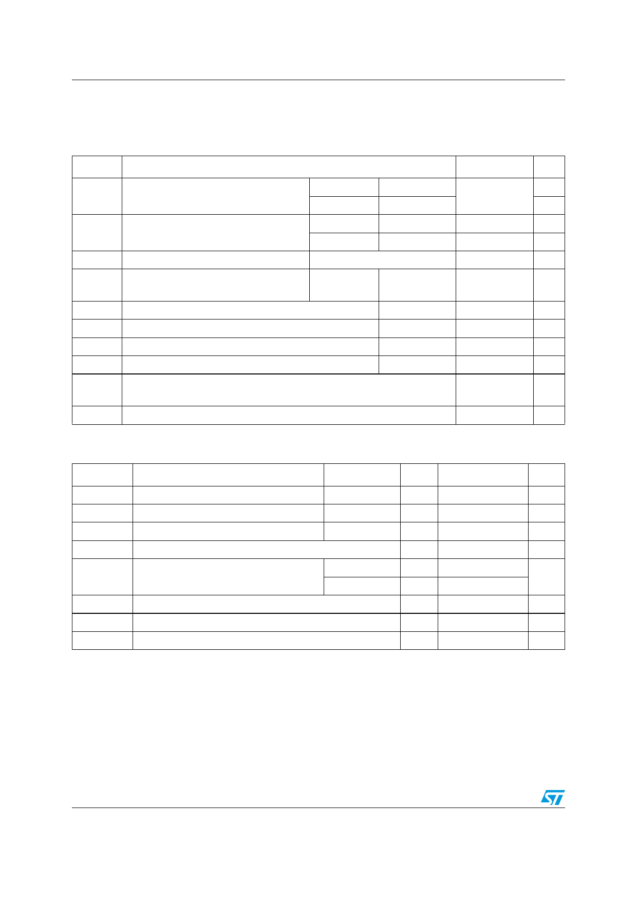
Table 1.
Symbol
Absolute maximum ratings (limiting values)
Parameter
Value
IT(RMS) RMS on-state current (full sine wave)
TO-220FPAB Tc = 105° C
DPAK
Tc = 110 °C
ITSM
Non repetitive surge peak on-state current F = 60 Hz
(full cycle sine wave, TJ initial = 25° C)
F = 50 Hz
t = 16.7 ms
t = 20 ms
I²t
I²t Value for fusing
tp = 10 ms
dI/dt
VPP (1)
Critical rate of rise of on-state current
IG = 2 x IGT, tr = 100 ns
Non repetitive line peak mains voltage (1)
F = 120 Hz
Tj = 125° C
Tj = 25° C
PG(AV) Average gate power dissipation
Tj = 125° C
PGM Peak gate power dissipation (tp = 20 µs)
Tj = 125° C
IGM Peak gate current (tp = 20 µs)
Tj = 125° C
Tstg Storage junction temperature range
Tj
Operating junction temperature range
Tl
Maximum lead soldering temperature during 10 s (at 3 mm from plastic case)
1. according to test described by IEC 61000-4-5 standard and Figure 16
2
8.4
8.0
0.5
50
2
0.1
10
1.6
-40 to +150
-40 to +125
260
Table 2. Electrical characteristics (Tj = 25° C, unless otherwise specified)
Symbol
Test conditions
Quadrant
Value
IGT(1)
VOUT = 12 V RL = 33 Ω
I - II - III
MAX
10
VGT
VOUT = 12 V RL = 33 Ω
I - II - III
MAX
1.1
VGD
IH (2)
VOUT = VDRM RL = 3.3 kΩ Tj = 125° C
IOUT = 100 mA
I - II - III
MIN
0.2
MAX
10
IL
IG = 1.2 x IGT
I - III
MAX
25
II
MAX
35
dV/dt (2) VOUT = 67% VDRM gate open Tj = 125° C
(dI/dt)c (2) (dV/dt)c = 15 V/µs Tj = 125° C
MIN
500
MIN
0.5
VCL
ICL = 0.1 mA tp = 1 ms Tj = 25° C
MIN
850
1. minimum IGT is guaranteed at 5% of IGT max
2. for both polarity of OUT pin referenced to COM pin
Unit
A
A
A²s
A/µs
kV
W
W
A
°C
°C
Unit
mA
V
V
mA
mA
V/µs
A/ms
V
2/11
Share Link: 