LTC1094 Просмотр технического описания (PDF) - Linear Technology
Номер в каталоге
Компоненты Описание
производитель
LTC1094 Datasheet PDF : 32 Pages
| |||
LTC1091/LTC1092
LTC1093/LTC1094
APPLICATI S I FOR ATIO
CS
DIN 1
DIN 2
DOUT 1
SHIFT MUX
ADDRESS IN
1 NULL BIT SHIFT A/D CONVERSION
RESULT OUT
DOUT 2
1091/2/3/4 AI01
the first CLK pulse enables DOUT. After one null bit, the A/D
conversion result is output on the DOUT line. Bringing CS
high resets the LTC1092 for the next data exchange.
2. Input Data Word
The LTC1092 requires no DIN word. It is permanently
configured to have a single differential input and to operate
in unipolar mode. The conversion result is output on the
DOUT line in MSB-first sequence, followed by LSB-first
sequence, providing easy interface to MSB- or LSB-first
serial ports. The following disussion applies to the con-
figuration of the LTC1091/LTC1093/LTC1094.
The LTC1091/LTC1093/LTC1094 clock data into the DIN
input on the rising edge of the clock. The input data words
are defined as follows:
LTC1091 DATA INPUT (DIN) WORD:
START
SGL/
DIFF
ODD/
SIGN
MSBF
MUX ADDRESS MSB-FIRST/
LSB-FIRST
LTC1093/LTC1094 DATA INPUT (DIN)WORD:
UNIPOLAR/
BIPOLAR
START
SGL/
DIFF
ODD/ SELECT SELECT
SIGN
1
0
MUX ADDRESS
UNI
MSBF
1091/2/3/4 AI02
MSB-FIRST/
LSB-FIRST
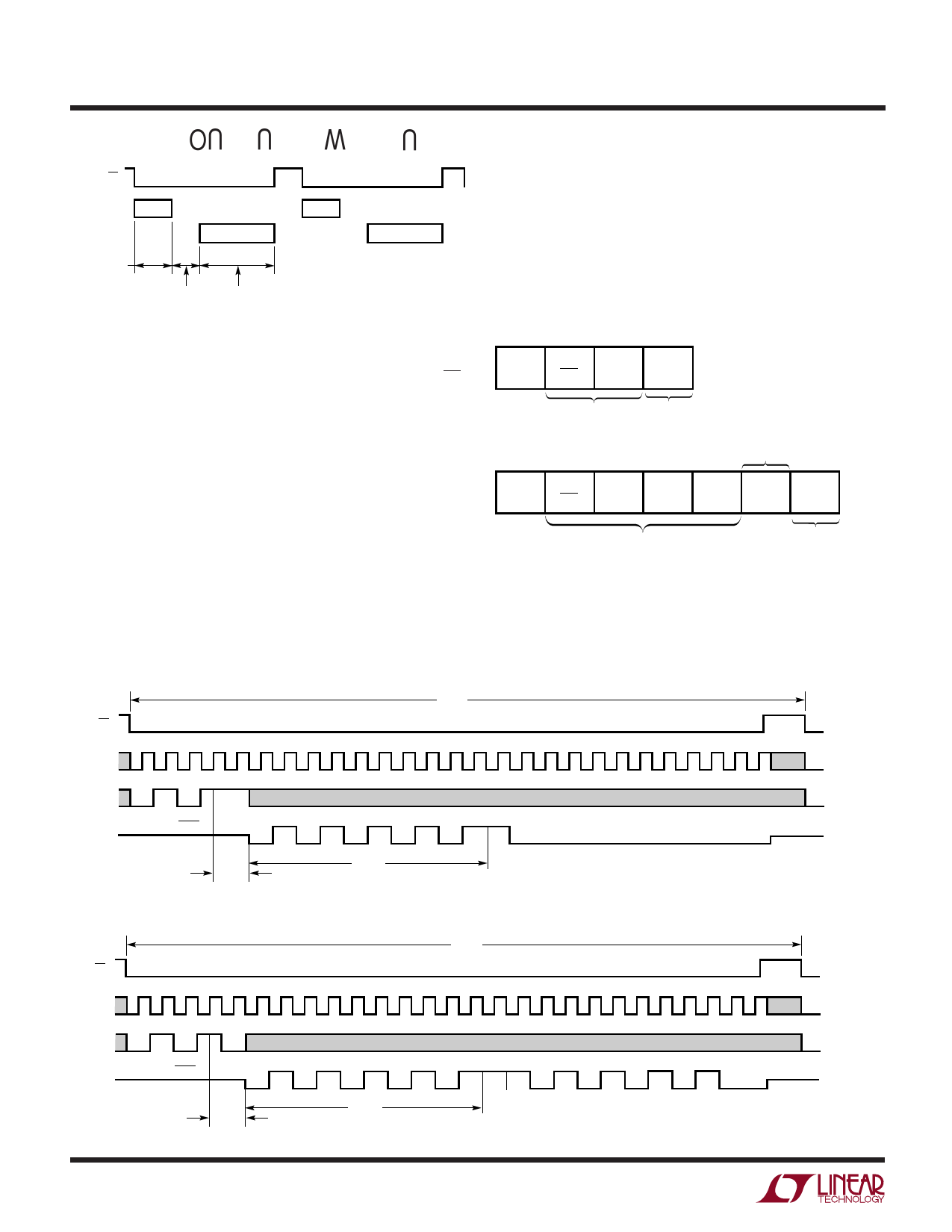
MSB-First Data (MSBF = 1)
CS
CLK
DIN
DOUT
START ODD/SIGN
SGL/ MSBF
Hi-Z DIFF
B9
tSMPL
LSB-First Data (MSBF = 0)
CS
CLK
DIN
DOUT
START ODD/SIGN
SGL/ MSBF
Hi-Z DIFF
B9
tSMPL
12
LTC1091 Operating Sequence
Example: Differential Inputs (CH1+, CH0 –)
tCYC
tCONV
DON’T CARE
B1 B0 FILLED WITH ZEROS
tCYC
tCONV
DON’T CARE
B1 B0 B1
Hi-Z
1091/2/3/4 AI03
Hi-Z
B9
FILLED WITH
ZEROS
1091/2/3/4 AI04
Share Link: 