AM29LV001BT-45RJIB Просмотр технического описания (PDF) - Advanced Micro Devices
Номер в каталоге
Компоненты Описание
производитель
AM29LV001BT-45RJIB
Advanced Micro Devices

AM29LV001BT-45RJIB Datasheet PDF : 40 Pages
| |||
TEST CONDITIONS
3.3 V
Device
Under
Test
CL
6.2 kΩ
2.7 kΩ
Note: Diodes are IN3064 or equivalent
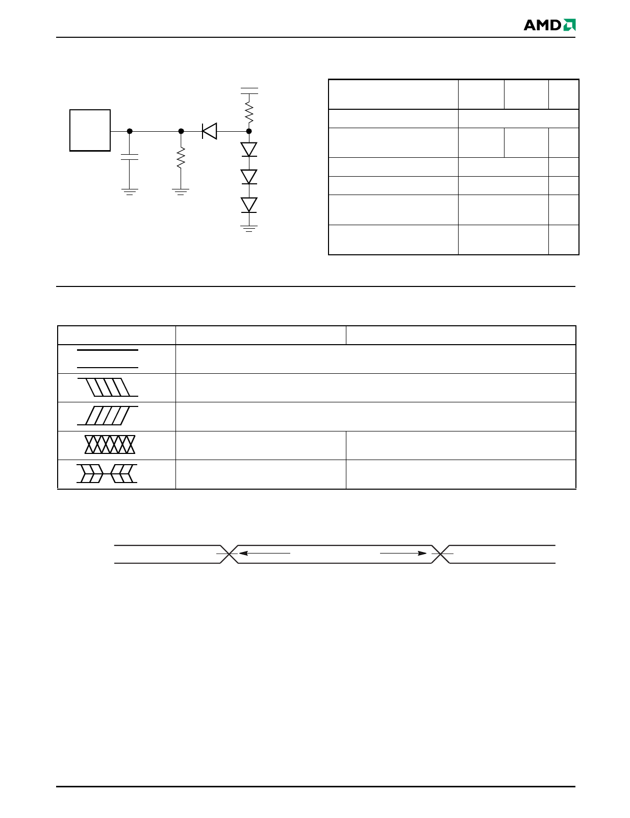
Figure 11. Test Setup
Table 7. Test Specifications
Test Condition
-45R,
-55
-70,
-90 Unit
Output Load
1 TTL gate
Output Load Capacitance, CL
(including jig capacitance)
30
100
pF
Input Rise and Fall Times
5
ns
Input Pulse Levels
0.0–3.0
V
Input timing measurement
reference levels
1.5
V
Output timing measurement
reference levels
1.5
V
KEY TO SWITCHING WAVEFORMS
WAVEFORM
INPUTS
Steady
OUTPUTS
Changing from H to L
Changing from L to H
Don’t Care, Any Change Permitted
Changing, State Unknown
Does Not Apply
Center Line is High Impedance State (High Z)
3.0 V
0.0 V
Input
1.5 V
Measurement Level
1.5 V
Figure 12. Input Waveforms and Measurement Levels
Output
September 26, 2002
Am29LV001B
25
Share Link: