2SJ540 Просмотр технического описания (PDF) - Renesas Electronics
Номер в каталоге
Компоненты Описание
производитель
2SJ540 Datasheet PDF : 8 Pages
| |||
2SJ540
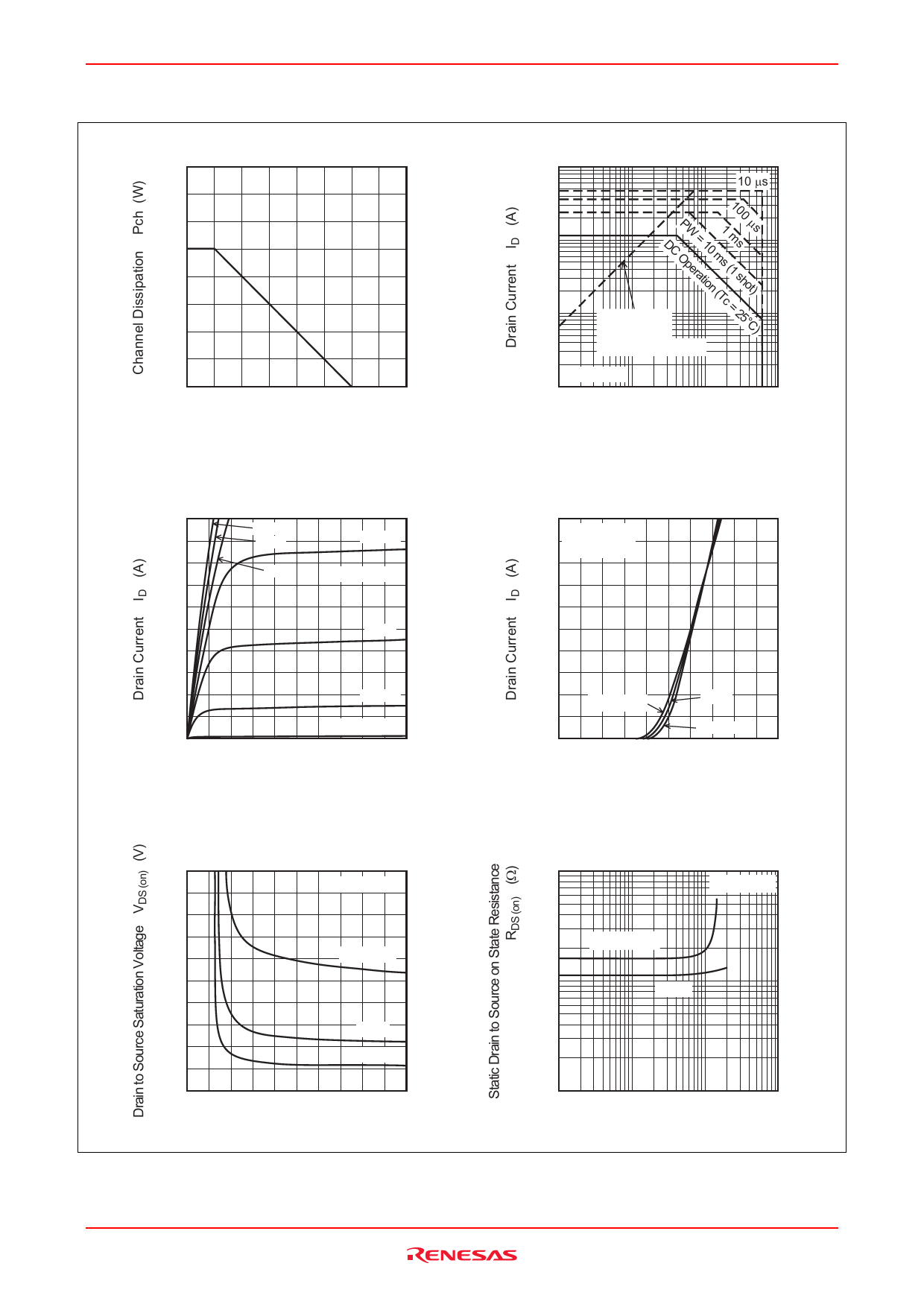
Main Characteristics
Power vs. Temperature Derating
80
60
40
20
0
0
50
100
150
200
Case Temperature Tc (°C)
Typical Output Characteristics
–10
–10 V
–5 V
–3.5 V
–8
–4 V
Pulse Test
–6
–3 V
–4
–2
–2.5 V
VGS = –2 V
0
0
–2 –4 –6 –8 –10
Drain to Source Voltage VDS (V)
Drain to Source Saturation Voltage vs.
Gate to Source Voltage
–1.0
Pulse Test
–0.8
–0.6
ID = –5 A
–0.4
–2 A
–0.2
–1 A
0
0
–4
–8 –12 –16 –20
Gate to Source Voltage VGS (V)
Rev.4.00 Jun 05, 2006 page 3 of 7
–100
–50
Maximum Safe Operation Area
10 µs
–20
–10
–5
–2
–1
–0.5
DC
Operation in
this area is
OPpWer=at1io0nm(Ts1c(=m1 2ss5h°oCt))
limited by RDS (on)
–0.2
Ta = 25°C
–0.1
–0.1 –0.3 –1 –3 –10 –30 –100
Drain to Source Voltage VDS (V)
Typical Transfer Characteristics
–10
VDS = –10 V
Pulse Test
–8
–6
–4
–2
Tc = 75°C
25°C
–25°C
0
0
–1 –2 –3 –4 –5
Gate to Source Voltage VGS (V)
Static Drain to Source on State Resistance
vs. Drain Current
1
Pulse Test
0.5
0.2
VGS = –4 V
0.1
–10 V
0.05
0.02
0.01
–0.1 –0.3 –1 –3 –10 –30 –100
Drain Current ID (A)
Share Link: 