M24SR –ü—Ä–ĺ—Ā–ľ–ĺ—ā—Ä —ā–Ķ—Ö–Ĺ–ł—á–Ķ—Ā–ļ–ĺ–≥–ĺ –ĺ–Ņ–ł—Ā–į–Ĺ–ł—Ź (PDF) - STMicroelectronics
–Ě–ĺ–ľ–Ķ—Ä –≤ –ļ–į—ā–į–Ľ–ĺ–≥–Ķ
–ö–ĺ–ľ–Ņ–ĺ–Ĺ–Ķ–Ĺ—ā—č –ě–Ņ–ł—Ā–į–Ĺ–ł–Ķ
–Ņ—Ä–ĺ–ł–∑–≤–ĺ–ī–ł—ā–Ķ–Ľ—Ć
M24SR
STMicroelectronics

M24SR Datasheet PDF : 90 Pages
| |||
M24SR02-Y
M24SR02-Y memory management
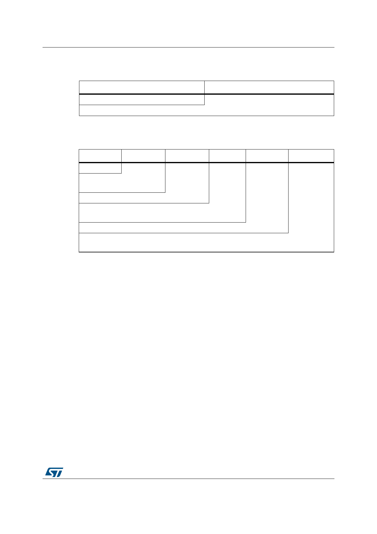
Table 10 gives some details about the ST reserved field.
0x0005
0x00
Table 10. Details about the ST reserved field
File offset
b7-b0
Table 11 gives some details about the RF enable field.
Table 11. Details about the RF enable field
File offset
b7
b6-b4
b3
b2-b1
b0
0x0006
0: the RF field is off (1)
1: the RF field is on (1)
RFU
0: the RF disable pad is at low state (1)
1: the RF disable pad is at high state (1)
RFU
0: the M24SR02-Y does not decode the command received from the RF interface
1: the M24SR02-Y decodes the command received from the RF interface
1. this field is written by the M24SR02-Y.
3.2
3.2.1
Read and write access rights to the memory
An NDEF file can be locked for read or write accesses. It is also protected by a 128-bit
password that the host shall present before accessing the NDEF file. There are two 128-bit
passwords, one for the read access and the other one for the write access.
An NDEF file can be permanently locked for read or write accesses. Thus, the host cannot
access the NDEF file.
The read password shall be sent to the M24SR02-Y device before reading a read-locked
NDEF file.
The write password shall be present on the M24SR02-Y device before writing a write-locked
NDEF file. The write password shall be sent to change the read or write access. The read or
write access right is defined for the NDEF file.
State of the Read and Write access rights
Two bytes in the CC file are used to define the Read and Write access rights to the NDEF
file. For more details, refer to Section 3.1.2: CC file layout.
DocID025386 Rev 10
25/90
28
Share Link: