AM29LV160BT-80FI Просмотр технического описания (PDF) - Advanced Micro Devices
Номер в каталоге
Компоненты Описание
производитель
AM29LV160BT-80FI
Advanced Micro Devices

AM29LV160BT-80FI Datasheet PDF : 46 Pages
| |||
PRELIMINARY
Addresses
(Word Mode)
40h
41h
42h
43h
44h
45h
46h
47h
48h
49h
4Ah
4Bh
4Ch
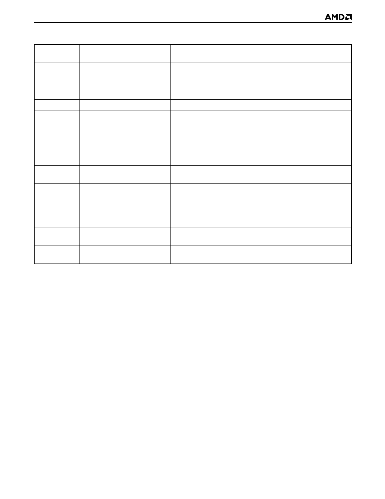
Table 8. Primary Vendor-Specific Extended Query
Addresses
(Byte Mode)
Data
Description
80h
0050h
82h
0052h
Query-unique ASCII string “PRI”
84h
0049h
86h
0031h
Major version number, ASCII
88h
0030h
Minor version number, ASCII
8Ah
0000h
Address Sensitive Unlock
0 = Required, 1 = Not Required
8Ch
0002h
Erase Suspend
0 = Not Supported, 1 = To Read Only, 2 = To Read & Write
8Eh
0001h
Sector Protect
0 = Not Supported, X = Number of sectors in per group
90h
0001h
Sector Temporary Unprotect
00 = Not Supported, 01 = Supported
Sector Protect/Unprotect scheme
92h
0004h
01 = 29F040 mode, 02 = 29F016 mode,
03 = 29F400 mode, 04 = 29LV800A mode
94h
0000h
Simultaneous Operation
00 = Not Supported, 01 = Supported
96h
0000h
Burst Mode Type
00 = Not Supported, 01 = Supported
98h
0000h
Page Mode Type
00 = Not Supported, 01 = 4 Word Page, 02 = 8 Word Page
Hardware Data Protection
The command sequence requirement of unlock cycles
for programming or erasing provides data protection
against inadvertent writes (refer to Table 9 for com-
mand definitions). In addition, the following hardware
data protection measures prevent accidental erasure
or programming, which might otherwise be caused by
spurious system level signals during VCC power-up
and power-down transitions, or from system noise.
Low VCC Write Inhibit
When VCC is less than VLKO, the device does not ac-
cept any write cycles. This protects data during VCC
power-up and power-down. The command register and
all internal program/erase circuits are disabled, and the
device resets. Subsequent writes are ignored until VCC
is greater than VLKO. The system must provide the
proper signals to the control pins to prevent uninten-
tional writes when VCC is greater than VLKO.
Write Pulse “Glitch” Protection
Noise pulses of less than 5 ns (typical) on OE#, CE# or
WE# do not initiate a write cycle.
Logical Inhibit
Write cycles are inhibited by holding any one of OE# =
VIL, CE# = VIH or WE# = VIH. To initiate a write cycle,
CE# and WE# must be a logical zero while OE# is a
logical one.
Power-Up Write Inhibit
If WE# = CE# = VIL and OE# = VIH during power up, the
device does not accept commands on the rising edge
of WE#. The internal state machine is automatically
reset to reading array data on power-up.
Am29LV160B
17
Share Link: