MAX1889 Просмотр технического описания (PDF) - Maxim Integrated
Номер в каталоге
Компоненты Описание
производитель
MAX1889 Datasheet PDF : 32 Pages
| |||
Triple-Output TFT LCD Power Supply
with Fault Protection
Input Capacitor
The input capacitor (CIN) reduces the current peaks
drawn from the input supply and reduces noise injection
into the device. Two 3.3µF ceramic capacitors are used
in the standard application circuit (Figure 1) because of
the high source impedance seen in typical lab setups.
Actual applications usually have much lower source
impedance since the step-up regulator typically runs
directly from the output of another regulated supply.
Typically, CIN can be reduced below the values used in
the standard applications circuit. Ensure a low noise sup-
ply at the IN pin by using adequate CIN. Alternatively,
greater voltage variation can be tolerated on CIN if IN is
decoupled from CIN using an RC lowpass filter (see R1,
C1 in Figure 1).
Rectifier Diode
The MAX1889’s high switching frequency demands a
high-speed rectifier. Schottky diodes are recommend-
ed for most applications because of their fast recovery
time and low forward voltage. In general, a 1A Schottky
diode complements the internal MOSFET well.
Input P-Channel MOSFET
Select the input P-channel MOSFET based on the cur-
rent rating, voltage rating, gate threshold, and on-resis-
tance. The MOSFET must be able to handle the peak
input current (see the Inductor Selection section). The
drain-to-source voltage rating of the input MOSFET
should be higher than the maximum input voltage.
Because the MOSFET conducts the full input current,
the on-resistance should be low enough for higher effi-
ciency. Use a low-threshold MOSFET to ensure that the
switch is fully enhanced at lowest input voltages.
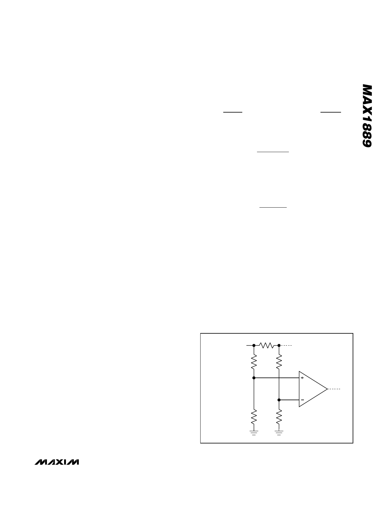
Setting the Input Overcurrent Threshold
The high-side comparator of the MAX1889 provides
input overcurrent protection when used in conjunction
with an external P-channel MOSFET P1. The accuracy
of the overcurrent threshold is affected by many fac-
tors, including comparator offset, resistor tolerance,
input voltage range, and variations in MOSFET
RDS(ON). The input overcurrent comparator is only
intended to protect against catastrophic failures. This
function is similar to an input fuse.
To minimize the impact of the comparator’s input offset
on the current-sense accuracy, the sense voltage
should be close to the upper limit of the common-mode
range, which extends up to 80% of the input voltage.
The resistive voltage-divider (R3/R4), combined with
the on-state resistance of P1, sets the overcurrent
threshold. The center of R3/R4 is connected to the
inverting input (OCN) as shown in Figure 6.
If the comparator and resistors are ideal, the threshold
is at the current where both inputs are equal:
( ) VIN
×
R2
R1+ R2
=
VIN -IL(MAX) × RDS(MAX)
× R4
R3 + R4
IL(MAX) is the average inductor current at maximum load
condition and minimum input voltage, and given by:
IL(MAX)
=
VOUT
η × VIN(MIN)
× ILOAD(MAX)
where η is the efficiency of the main step-up regulator.
If the step-up regulator’s minimum input voltage is 2.7V,
output voltage is 9V and maximum load current is 0.3A.
Assuming 80% efficiency, the maximum average induc-
tor current is:
IL(MAX)
=
9V
0.8 × 2.7V
× 0.3A
= 1.25A
RDS(MAX) is the maximum on-state drain-to-source
resistance of P1. The maximum RDS(ON) at +25°C can
be found in the MOSFET data sheet, but that number
does not include the temperature coefficient.
Since the temperature coefficient for the resistance is
0.5%/°C, RDS(MAX) can be calculated with the following
equation:
[ ] ( ) RDS(MAX) = RDS_25°C × 1+ 0.005 × TJ - 25
where TJ is the actual MOSFET junction temperature in
normal operation due to ambient temperature rise and
self-heating caused by power dissipation. As an exam-
ple, consider Fairchild FDN304P, which has a maxi-
mum RDS(ON) at room temperature of 70mΩ.
RDS(ON)
VIN
R1
R3
OCP
OCN
OC COMP
R2
R4
Figure 6. Setting the Overcurrent Threshold
______________________________________________________________________________________ 19
Share Link: 