L4992 Просмотр технического описания (PDF) - STMicroelectronics
Номер в каталоге
Компоненты Описание
производитель
L4992 Datasheet PDF : 26 Pages
| |||

L4992
DESIGN PROCEDURE (continued)
Pulse-skipping operation is enabled by default in order to maximize efficiency also in low load current
range. The transition between PWM and pulse-skipping occurs approximately below 1A, however there
is a region in which the two operation modes coexist rather than a definite boundary. That can be seen
on the scope as an irregularity of the waveforms but does not have much influence both on output ripple
and efficiency.
Those who do not appreciate asynchronous operation of the pulse-skipping mode can disable it for both
regulators, by setting switch 2 on 1. That maintains PWM operation up to very low output currents where,
however, the regulation becomes incompatible with the switching frequency. This means that the mini-
mum ON-time of the high-side MOSFET is too long for the thruput energy level at the operating fre-
quency. Thus the control system begins skipping conduction cycles to avoid the output voltage drifting
upwards.
Table 1 shows the complete L4992 EVAL KIT parts list. Critical components characteristics are given in
detail.
DEMO BOARD EVALUATION
The following diagrams and tables show the typical performance of the demonstration board in terms of
efficiency, line regulation and load regulation. The 12V linear regulator and REG5 are also characterized.
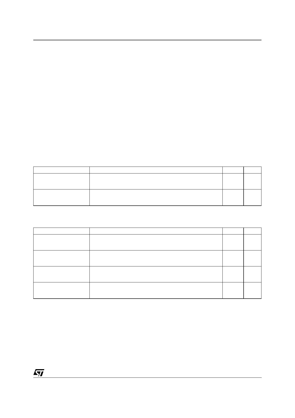
Table 2: PWM Regulators: Optimum Efficiency
Parameter
+3.3V Maximum Efficiency
+5.1V Maximum Efficiency
Test Condition
RUN3 = RUN5 = HIGH, NOSKIP = LOW
Vin = 6V, Iout = 0.5 A, fSW = 200 kHz
Vin = 6V, Iout = 1A, fSW = 300 kHz
RUN3 = LOW, NOSKIP = LOW
Vin = 6V, Iout = 1A, fSW = 200 kHz
Vin = 6V, Iout = 1A, fSW = 300 kHz
Value Unit
%
95.2
94.6
%
96.4
95.8
Table 3: PWM regulators: Line and Load Regulation.
Parameter
+3.3V Line Regulation
+5.1V Line Regulation
+3.3V Load Regulation
+5.1V Load Regulation
Test Condition
RUN5 = LOW, NOSKIP = LOW, 6 < Vin < 20V
Iout = 0.1 A, fSW = 200 kHz
Iout =1A, fSW = 200 kHz
RUN3 = LOW, NOSKIP = LOW, 6 < Vin < 20V
Iout = 0.1A, fSW = 200 kHz
Iout = 1A, fSW = 200 kHz
RUN5 = LOW, NOSKIP = LOW, 5 mA < Iout < 3A
Vin = 6 V, fSW = 200 kHz
Vin = 15V, fSW = 200 kHz
RUN3 = LOW, NOSKIP = LOW, 5 mA < Iout < 3A
Vin = 6 V, fSW = 200 kHz
Vin = 15V, fSW = 200 kHz
Value Unit
mV
2
15
mV
3
20
mV
85
70
mV
90
75
21/26