CXD2498 Просмотр технического описания (PDF) - Sony Semiconductor
Номер в каталоге
Компоненты Описание
производитель
CXD2498 Datasheet PDF : 51 Pages
| |||
CXD2498R
Serial interface clock internal loading characteristics (2)
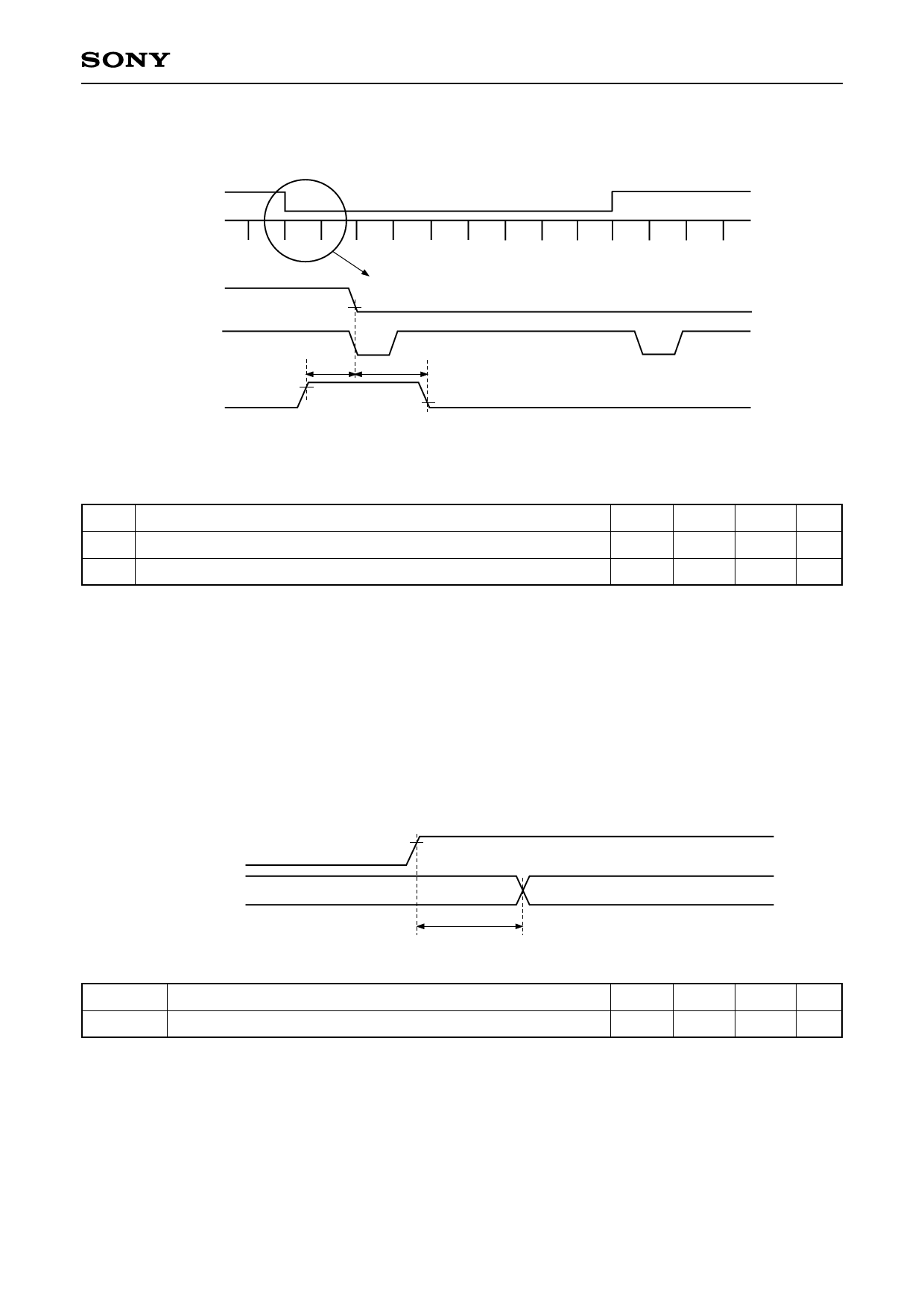
Example: During frame mode
VD
HD
Enlarged view
VD
HD
SEN
0.2VDDc
ts1
0.8VDDc
th1
0.2VDDc
∗ Be sure to maintain a constantly high SEN logic level near the falling edge of VD.
(Within the recommended operating conditions)
Symbol
Definition
ts1 SEN setup time, activated by the falling edge of VD
th1 SEN hold time, activated by the falling edge of VD
Min. Typ. Max. Unit
0
ns
200
ns
∗ Restriction with an operating frequency of 22.5MHz.
Serial interface clock output variation characteristics
Normally, the serial interface data is loaded to the CXD2498R at the timing shown in “Serial interface clock
internal loading characteristics (1)” above. However, one exception to this is when the data such as STB is
loaded to the CXD2498R and controlled at the rising edge of SEN. See ”Description of Operation”.
SEN
0.8VDDc
Output signal
tpdPULSE
(Within the recommended operating conditions)
Symbol
Definition
tpdPULSE Output signal delay, activated by the rising edge of SEN
Min. Typ. Max. Uniy
5
70 ns
– 11 –
Share Link: 