HIP1015CB(2000) Просмотр технического описания (PDF) - Intersil
Номер в каталоге
Компоненты Описание
производитель
HIP1015CB Datasheet PDF : 10 Pages
| |||
HIP1015, HIP1016
Typical Performance Curves (Continued)
+350V
VDRAIN 50V/DIV
IOUT 1A/DIV
+350V
VDRAIN 50V/DIV
IOUT 1A/DIV
VGATE 5V/DIV
PWRON 5V/DIV
0V
2ms/DIV
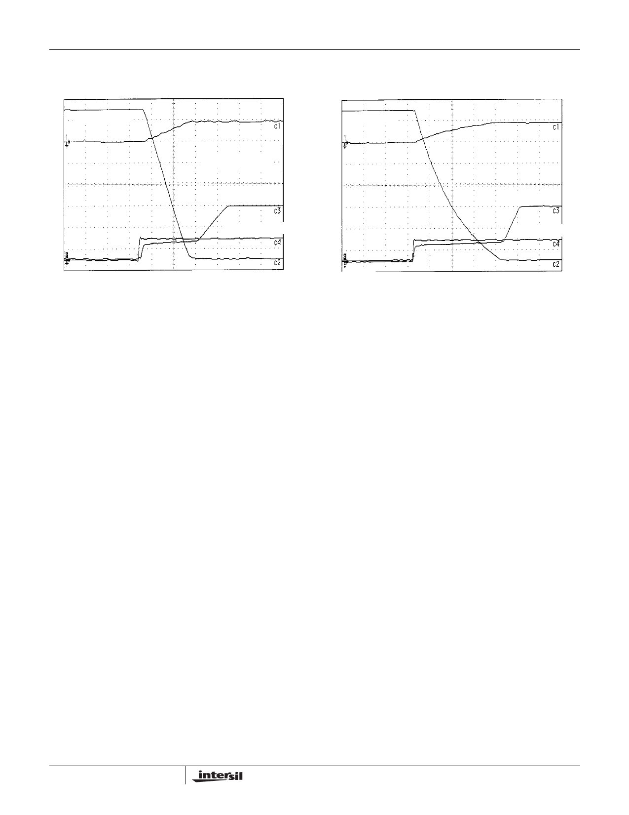
FIGURE 15. +350V LOW SIDE SWITCHING CGATE = 100pF
HIP1015EVAL1 Board
The HIP1015EVAL1 is configured as a +12V high side
switch controller with the OC latch-off level set at ~1.5A.
(See Figure 16. for HIP1015EVAL1 schematic and Table 4.
for BOM.) Bias and load connection points are provided
along with test points for each IC pin. Also included with the
HIP1015EVAL1 board is one loose packed HIP1016 for 5V
bus switching evaluation.
With the chip to be biased from the +12V bus being
switched, through B2, GND B5, the load connected between
B3 and B4 and with jumper J1 installed the HIP1015 can be
evaluated. PWRON pin pulls high enabling HIP1015 if not
driven low.
With the 750Ω Overcurrent Voltage Threshold set resistor
(R2) the OC Vth is set to 15mV and with the 10mΩ sense
resistor the HIP1015EVAL1 has a nominal OC trip level of
1.5A. The 0.047µF delay time to latch-off capacitors results
in a nominal 4.4ms before latch-off of outputs after an OC
event.
HIP1016EVAL1 Board
The HIP1016EVAL1 is default configured as a negative
voltage low side switch controller with a ~2.4A OC latch-off
level. (See Figure 17 for HIP1016EVAL1 schematic and
Table 4 for BOM and component description.) This basic
configuration is capable of controlling both larger positive or
negative potential voltages with minimal changes.
Bias and load connection points are provided in addition to
test points, TP1-8 for each IC pin. The terminals, J1 and J4
are for the bus voltage and return, respectively, with the
more negative potential being connected to J4. With the load
between terminals J2 and J3 the board is now configured for
8
VGATE 5V/DIV
PWRON 5V/DIV
0V
2ms/DIV
FIGURE 16. +350V LOW SIDE SWITCHING CGATE = 1000pF
evaluation. The device is enabled through LOGIN, TP9 with
a TTL signal. HIP1016EVAL1 includes a level shifting circuit
with an opto-coupling device for the PWRON input so that
standard TTL logic can be translated to the -V reference for
chip control.
When controlling a positive voltage, PWRON can be
accessed at TP8.
The HIP1016EVAL1 is provided with a high voltage linear
regulator for convenience to provide chip bias from +/-24V to
+/-350V. This can be removed and replaced with the zener &
resistor bias scheme as discussed earlier. High voltage
regulators are no longer available from Intersil but can be
purchased from other IC manufacturers.
Reconfiguring the HIP1016EVAL1 board for increased OC
latch-off can be done by changing the RSENSE and RISET
resistor values as the provided FET is 75A rated. If
evaluation at > 60V, an alternate FET must be chosen with
an adequate BVDSS. Table 3 below provides a sample of
Intersil Power MOSFET offerings for various bus voltages.
TABLE 4. MOSFETs FOR EVALUATED VBUS VOLTAGE
+/-VBUS
24V HUF76145
MOSFET
36V HUF75345
48V HUF75545, HUF75542
72V HUF75645
140V IRF646, IRFR214
350V IRFP450
Share Link: 