CXG1030N Просмотр технического описания (PDF) - Sony Semiconductor
Номер в каталоге
Компоненты Описание
производитель
CXG1030N Datasheet PDF : 5 Pages
| |||
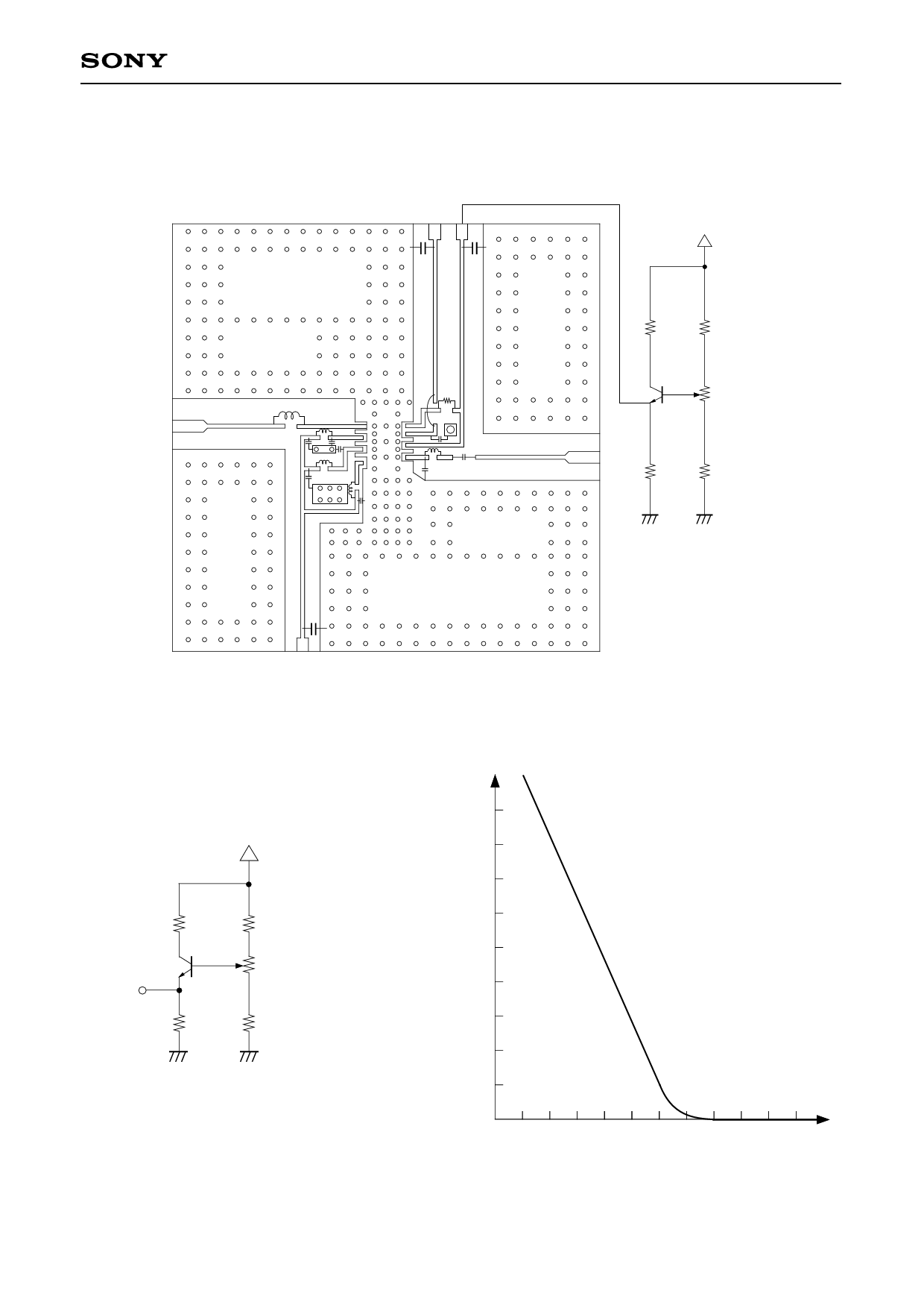
Recommended Evaluation Circuit
CXG1030N
RFIN
GND
VCTL
VGG2
C2
C2
3.0V
100Ω
6.8kΩ
L4
L1
C2
C2
C1
C2 L2
L3
C3
1kΩ
C1
L5 C1
C4
Via Hole
Variable
resistor RV
10kΩ (Max.)
RFOUT
1kΩ
180Ω
GND
C2
Glass fabric-base epoxy board
GND for the overall back side
Dimension : 5cm × 5cm
Thickness : 0.2mm
VDD C1=100pF C2=1nF C3=10nF C4=1pF
L1=18nH L2=10nH L3=1.8nH L4=3.9nH L5=2.7nH
Recommended Gate Bias Circuit and
Circuit Characteristics
3.0V
VGG2
100Ω
6.8kΩ
RV1 Variable
RV2
resistor RV
10kΩ (Max.)
1kΩ
180Ω
(V)
VGG2
0.5
0
5
10
RV1 (V)
Application circuits shown are typical examples illustrating the operation of the devices. Sony cannot assume responsibility for
any problems arising out of the use of these circuits or for any infringement of third party patent and other right due to same.
—3—
Share Link: 