AD9430/PCB-CMOS Просмотр технического описания (PDF) - Analog Devices
Номер в каталоге
Компоненты Описание
производитель
AD9430/PCB-CMOS Datasheet PDF : 20 Pages
| |||
PRELIMINARY TECHNICAL DATA
AD9430
Digital Outputs
The off chip drivers on the chip can be configured by the
user to provide CMOS or LVDS compatible output levels
via pin S2.
The CMOS digital outputs (S2=0) are TTL/CMOS-
compatible for lower power consumption. The outputs are
biased from a separate supply (VDD), allowing easy
interface to external logic. The outputs are CMOS devices
which will swing from ground to VDD (with no dc load). It
is recommended to minimize the capacitive load the ADC
drives by keeping the output traces short (<1 inch, for a total
CLOAD < 5 pF). When operating in cmos mode it is also
recommended to place low value (220 ohm) series damping
resistors on the data lines to reduce switching transient
effects on performance.
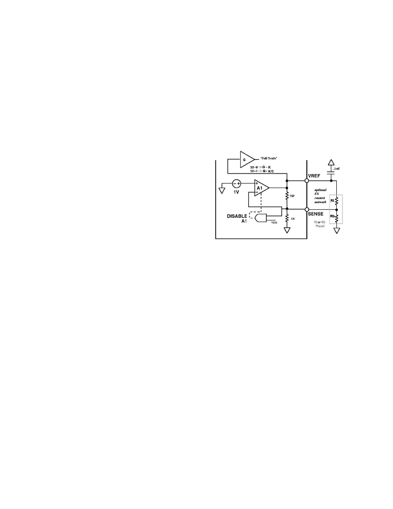
Voltage Reference
A stable and accurate 1.25 V voltage reference is built into
the AD9430 (VREF). The analog input Full Scale Range is
linearly proportional to the voltage at VREF. VREF (and in
turn input full scale ) can be varied by adding an external
resistor network at VREF, SENSE and GROUND. (See
figure X ) . No appreciable degradation in performance
occurs when VREF is adjusted ±5%. Note that an external
reference can be used by connecting the SENSE pin to VDD
(disabling internal reference) and driving VREF with the
external reference source. A .1uF capacitor to ground is
recommended at VREF pin in internal and external reference
applications.
LVDS outputs are available when S2=VDD and a 3.7K
RSET resistor is placed at pin 7 ( LVDSBIAS) to ground .
This resistor sets the output current at each output equal to a
nominal 3.5mA ( 10* IRSET) . A 100 ohm differential
termination resistor placed at the lvds receiver inputs results
in a nominal 350mV voltage swing at the receiver. Note that
when operating in LVDS mode the output supply must be at
a dc potential greater than or equal to the analog supply level
(AVDD). This can be accomplished simply by biasing the
two supplies from the same power plane or by tying the two
supplies on the pcb through an inductor. When operating in
CMOS mode this is not required and separate supplies are
recommended.
Simplified Voltage Reference Equivalent Circuit
Clock Outputs (DCO+, DCO-)
The input ENCODE is divided by two (in CMOS mode) and
available off-chip at DCO+ and DCO-. These clocks can
facilitate latching off-chip, providing a low skew clocking
solution (see timing diagram). The on-chip clock buffers
should not drive more than 5 pF of capacitance to limit
switching transient effects on performance.
Note that the Outputs clocks are CMOS levels when CMOS
mode is selected(S2=0) and are LVDS levels when in LVDS
mode(S2=VDD). (Requiring a 100ohm differential
termination at receiver in LVDS mode). The output clock in
LVDS mode switches at the encode rate.
REV. PrG 4/01/2002
-13-
Share Link: 