ADV476KP35 Просмотр технического описания (PDF) - Analog Devices
Номер в каталоге
Компоненты Описание
производитель
ADV476KP35 Datasheet PDF : 12 Pages
| |||
ADV476
ABSOLUTE MAXIMUM RATINGS1
VCC to GND . . . . . . . . . . . . . . . . . . . . . . . . . . . . . . . . . . +7 V
Voltage on any Digital Pin . . . . . GND – 0.5 V to VCC + 0.5 V
Ambient Operating Temperature (TA) . . . . . –55°C to +125°C
Storage Temperature (TS) . . . . . . . . . . . . . . –65°C to +150°C
Junction Temperature (TJ) . . . . . . . . . . . . . . . . . . . . +150°C
Lead Temperature (Soldering, 10 secs) . . . . . . . . . . . +300°C
Vapor Phase Soldering (1 minute) . . . . . . . . . . . . . . . +220°C
Red, Green, Blue to GND2 . . . . . . . . . . . . . . . . . . 0 V to VCC
NOTES
1Stresses above those listed under “Absolute Maximum Ratings” may cause
permanent damage to the device. This is a stress rating only and functional
operation of the device at these or any other conditions above those listed in the
operational sections of this specification is not implied. Exposure to absolute
maximum rating conditions for extended periods may affect device reliability.
2Analog output short circuit to any power supply or common can be of an indefinite
duration.
Model
ORDERING GUIDE1, 2
Speed Package Type
Package
Option3
ADV476KN35
ADV476KN50
ADV476KN66
ADV476KP35
ADV476KP50
ADV476KP66
35 MHz
50 MHz
66 MHz
35 MHz
50 MHz
66 MHz
28-Pin DIP
28-Pin DIP
28-Pin DIP
44-Pin PLCC
44-Pin PLCC
44-Pin PLCC
N-28
N-28
N-28
P-44A
P-44A
P-44A
NOTES
1All devices are specified for 0°C to +70°C operation.
2Devices are packaged in 0.6" 28-pin plastic DIPs (N-28), and 44-pin J-leaded
PLCC (P-44A).
3N = Plastic DIP; P = Plastic Leaded Chip Carrier.
RECOMMENDED OPERATING CONDITIONS
Parameter
Symbol Min Typ Max Units
Power Supply
VCC
Ambient Operating Temperature TA
Output Load
RL
Reference Current
IREF
4.5 5.00 5.5 Volts
0
+70 °C
37.5
Ω
–3
–10 mA
CAUTION
ESD (electrostatic discharge) sensitive device. Electrostatic charges as high as 4000 V readily
accumulate on the human body and test equipment and can discharge without detection.
Although the ADV476 features proprietary ESD protection circuitry, permanent damage may
occur on devices subjected to high energy electrostatic discharges. Therefore, proper ESD
precautions are recommended to avoid performance degradation or loss of functionality.
WARNING!
ESD SENSITIVE DEVICE
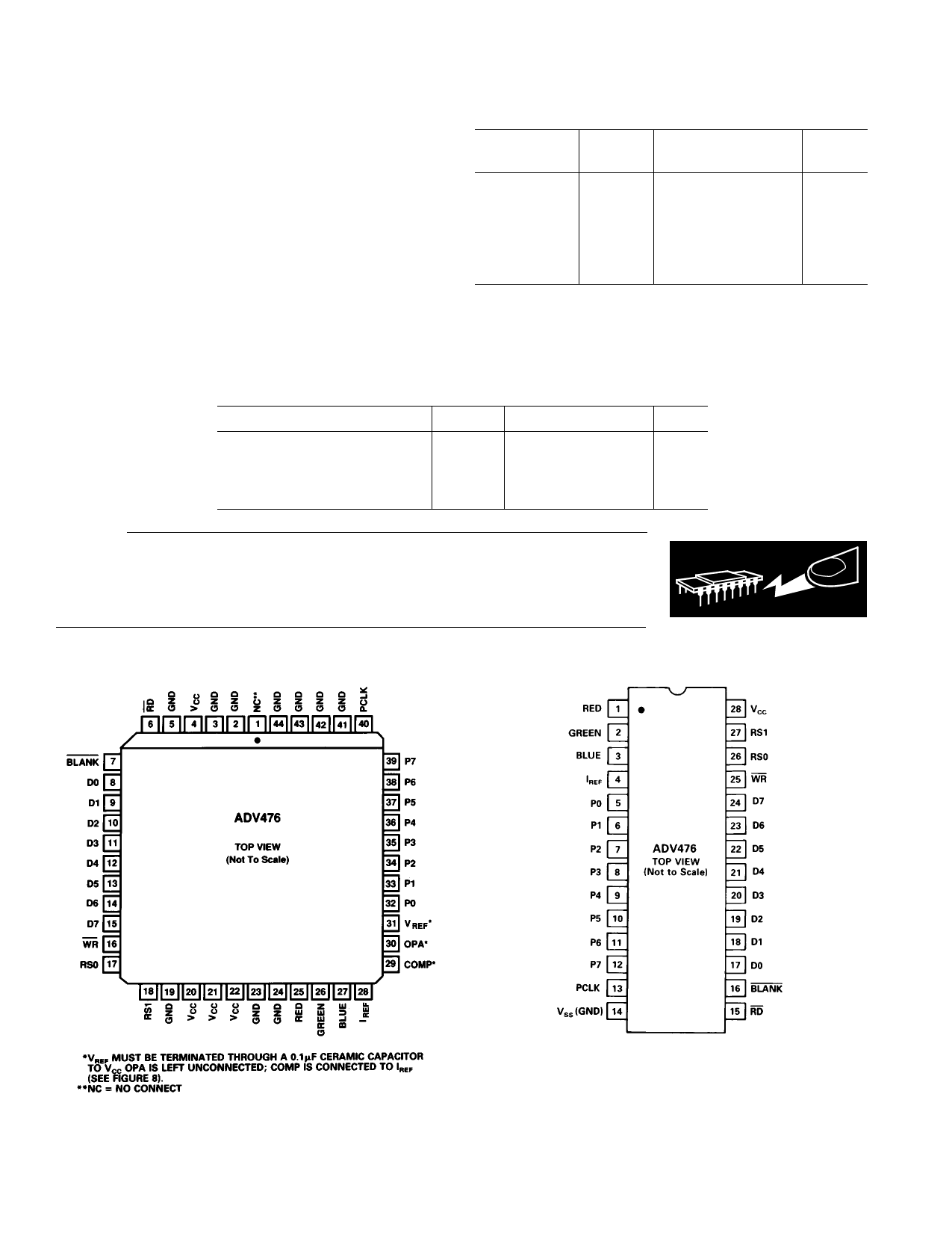
PIN CONFIGURATIONS
PLCC
DIP
The above pins allow the ADV476KP (44-Pin PLCC) to be al-
ternatively driven by a voltage reference. If it is desired to use a
voltage reference configuration instead of the current reference
configuration described in this data sheet, the above listed pins
must be connected as described in Figure 6 of the ADV478/
ADV471 data sheet of this reference manual.
–4–
REV. B
Share Link: 