PCA9556(1998) Просмотр технического описания (PDF) - Philips Electronics
Номер в каталоге
Компоненты Описание
производитель
PCA9556 Datasheet PDF : 12 Pages
| |||
Philips Semiconductors
Octal SMBus Registered Interface
Product specification
PCA9556
FEATURES
• SMBus compliance with fixed 3.3V voltage levels
• Operating power supply voltage range of 3.0V – 3.6V
• Active high polarity inverter register
• Write protect register
• Active low reset pin
• Low leakage current on power-down
• Noise filter on SCL/SDA inputs
• No glitch on power-up
• Internal power-on reset
• 8 I/O pins which default to 8 inputs
• High impedance open drain on I/O
DESCRIPTION
The PCA9556 is a silicon CMOS circuit which provides parallel
input/output expansion for SMBus applications. The PCA9556
consists of an 8-bit input port register, 8-bit output port register, and
an SMBus interface. It has low current consumption and a high
impedance open drain output pin, I/O0.
The SMBus system master can reset the PCA9556 in the event of a
timeout by asserting a LOW on the reset input. The SMBus system
master can also invert the PCA9556 inputs by writing to their active
HIGH polarity inversion bits. Finally, the SMBus system master can
enable the PCA9556’s I/Os as either inputs or outputs by writing to
their I/O configuration bits.
The power-on reset sets the registers to their default values and
initializes the SMBus state machine. The RESET pin causes the
same reset/initialization to occur without depowering the part.
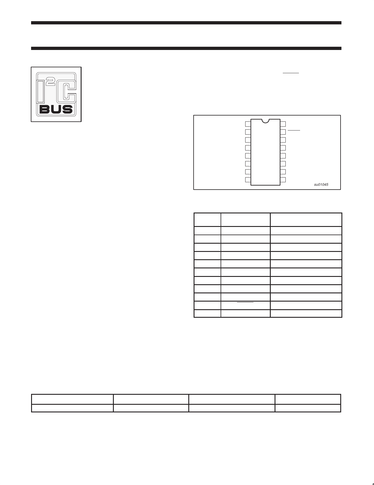
PIN CONFIGURATION
SCL 1
SDA 2
A0 3
A1 4
A2 5
I/O0 6
I/O1 7
VSS 8
16 VDD
15 RESET
14 I/O7
13 I/O6
12 I/O5
11 I/O4
10 I/O3
9 I/O2
su01045
Figure 1. Pin configuration
PIN DESCRIPTION
PIN
NUMBER
SYMBOL
1
SCL
2
SDA
3
A0
4
A1
5
A2
6
I/O0
7
I/O1
8
VSS
9
I/O2
10
I/O3
11
I/O4
12
I/O5
13
I/O6
14
I/O7
15
RESET
16
VDD
FUNCTION
Serial clock line
Serial data line
Address input 0
Address input 1
Address input 2
I/O0 (open drain)
I/O1
Supply GROUND
I/O2
I/O3
I/O4
I/O5
I/O6
I/O7
External reset (active LOW)
Supply voltage
ORDERING INFORMATION
PACKAGES
16-Pin Plastic TSSOP16 Type I
TEMPERATURE RANGE
0°C to +70°C
OUTSIDE NORTH AMERICA
PCA9556 PW
DRAWING NUMBER
SOT403-1
1998 Dec 18
2
853-2138 20549
Share Link: 