NX3V1T66_08 Просмотр технического описания (PDF) - NXP Semiconductors.
Номер в каталоге
Компоненты Описание
производитель
NX3V1T66_08 Datasheet PDF : 18 Pages
| |||
NXP Semiconductors
NX3V1T66
Low-voltage analog switch
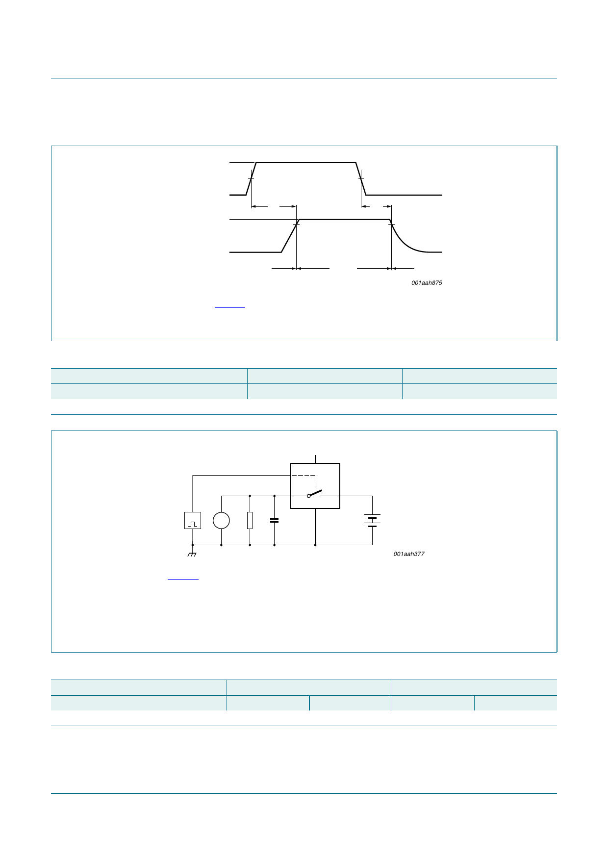
12.1 Waveform and test circuits
VI
E input
GND
VOH
Y output
OFF to HIGH
HIGH to OFF
GND
VM
ten
switch
disabled
tdis
VX
switch
enabled
Measurement points are given in Table 10.
Logic level: VOH is the typical output voltage that occurs with the output load.
Fig 14. Enable and disable times
VX
switch
disabled
001aah875
Table 10. Measurement points
Supply voltage
VCC
1.4 V to 3.6 V
Input
VM
0.5VCC
Output
VX
0.9VOH
VCC
E
Y/Z
Z/Y
G VI V VO
RL
CL
Test data is given in Table 11.
Definitions test circuit:
RL = Load resistance.
CL = Load capacitance including jig and probe capacitance.
VEXT = External voltage for measuring switching times.
Fig 15. Load circuit for switching times
Table 11. Test data
Supply voltage
VCC
1.4 V to 3.6 V
Input
VI
VCC
tr, tf
≤ 2.5 ns
VEXT = 1.5 V
001aah377
Load
CL
35 pF
RL
50 Ω
NX3V1T66_2
Product data sheet
Rev. 02 — 24 July 2008
© NXP B.V. 2008. All rights reserved.
9 of 18
Share Link: 