CGY81 Просмотр технического описания (PDF) - Siemens AG
Номер в каталоге
Компоненты Описание
производитель
CGY81 Datasheet PDF : 12 Pages
| |||
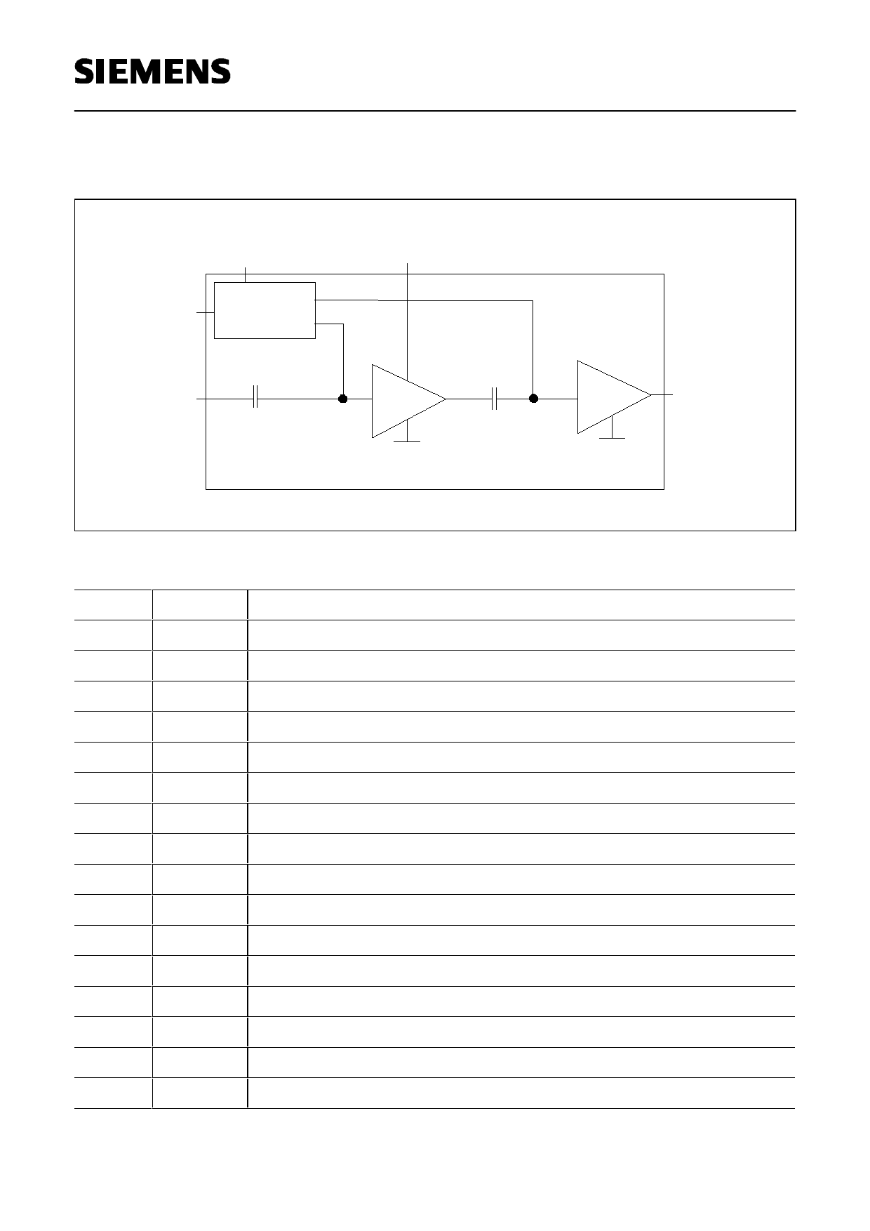
Functional Block Diagram:
Vneg
VD1
Vcon
Control
Circuit
RF IN
CGY 81
RF OUT
Pin Configuration:
Pin #
1
2
3
4
5
6
7
8
9
10
11
12
13
14
15
16
Name Configuration
VD Cell Drain voltage preamplifier stage
n. c.
RF IN Cell RF IN
n. c.
Vneg Negative voltage
Vcon Control voltage
n. c.
n. c.
n. c.
n. c.
RF out RF out / drain voltage final stage
RF out RF out / drain voltage final stage
RF out RF out / drain voltage final stage
RF out RF out / drain voltage final stage
n. c.
n. c.
Siemens Aktiengesellschaft
2
Semiconductor Group
2
23.07.98
HL HF PE 1G9a9A8s-111/-F0o1
Share Link: 