MAX4800CXZ(2009) Просмотр технического описания (PDF) - Maxim Integrated
Номер в каталоге
Компоненты Описание
производитель
MAX4800CXZ Datasheet PDF : 16 Pages
| |||
Low-Charge Injection,
8-Channel, High-Voltage Analog Switches
MAX4802
TQFP
1
2, 4, 6, 7, 9,
11,13, 15, 17,
19, 21, 23, 26,
30, 31, 32, 38,
40, 42, 44, 46,
48
3
5
8
10
12
14
16
18
20
22
24
PIN
MAX4802
CSBGA
E4
—
E1
E3
D1
D3
D4
C3
C4
A4
C5
D5
C6
25
C7
27
D6
28
D7
29
D9
33
E9
34
E7
35
E6
36
F7
37
F6
39
E5
41
F5
43
F4
45
H4
47
F3
MAX4802
PLCC
26
9, 15
27
28
1
2
3
4
5
6
7
8
10
12
11
13
14
16
17
18
19
20
21
22
23
24
25
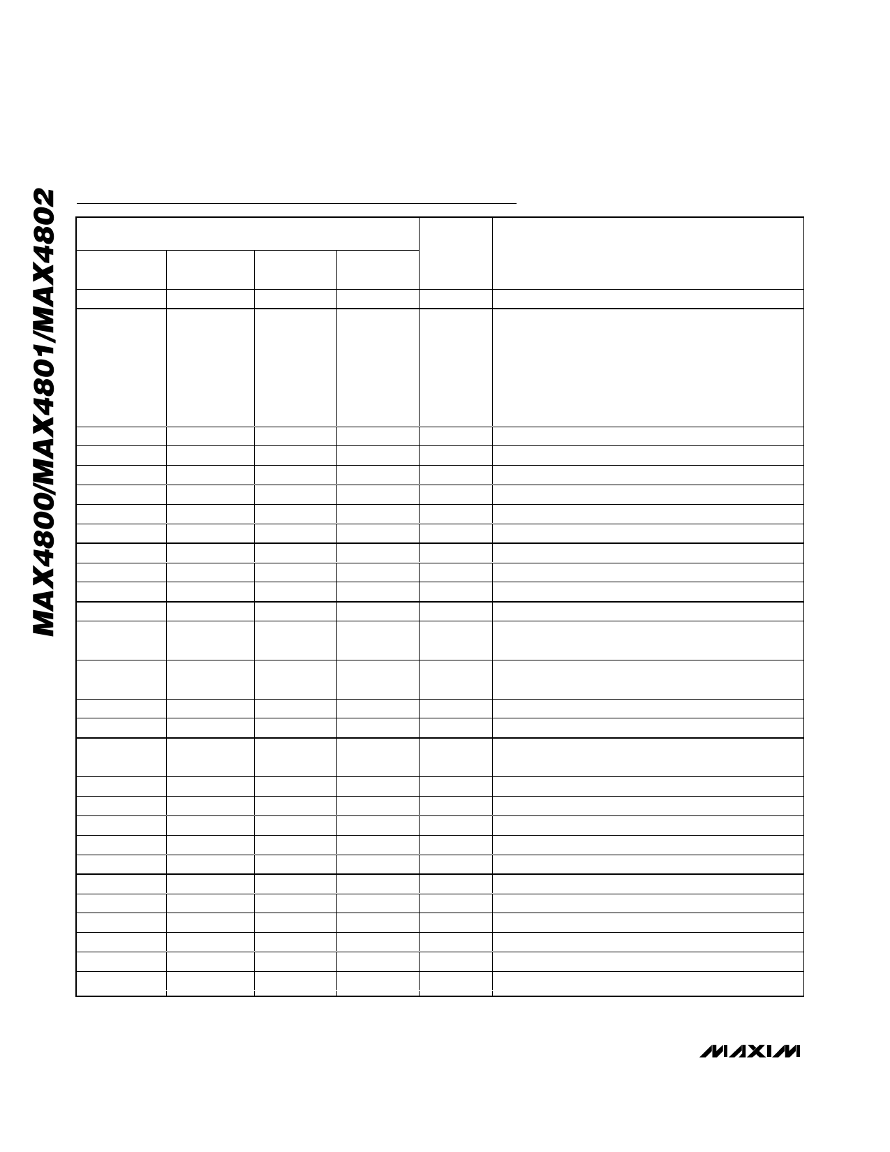
Pin Descriptions (continued)
NAME
FUNCTION
COM5 Analog Switch 5 – Common Terminal
N.C.
Not Connected Internally
COM4
NO4
COM3
NO3
COM2
NO2
COM1
NO1
COM0
NO0
VPP
VNN
RGND
GND
VDD
DIN
CLK
LE
CLR
DOUT
COM7
NO7
COM6
NO6
NO5
Analog Switch 4 – Common Terminal
Analog Switch 4 – Normally Open Terminal
Analog Switch 3 – Common Terminal
Analog Switch 3 – Normally Open Terminal
Analog Switch 2 – Common Terminal
Analog Switch 2 – Normally Open Terminal
Analog Switch 1 – Common Terminal
Analog Switch 1 – Normally Open Terminal
Analog Switch 0 – Common Terminal
Analog Switch 0 – Normally Open Terminal
Positive High-Voltage Supply. Bypass VPP to GND with a
0.1μF or greater ceramic capacitor.
Negative High-Voltage Supply. Bypass VNN to GND with a
0.1μF or greater ceramic capacitor.
Bleed Resistor Ground
Ground
Digital-Supply Voltage. Bypass VDD to GND with a 0.1μF or
greater ceramic capacitor.
Serial Data Input
Serial Clock Input
Latch Enable Input, Active Low
Latch Clear Input
Serial Data Output
Analog Switch 7 – Common Terminal
Analog Switch 7 – Normally Open Terminal
Analog Switch 6 – Common Terminal
Analog Switch 6 – Normally Open Terminal
Analog Switch 5 – Normally Open Terminal
8 _______________________________________________________________________________________
Share Link: 