CM1220 Просмотр технического описания (PDF) - ON Semiconductor
Номер в каталоге
Компоненты Описание
производитель
CM1220 Datasheet PDF : 6 Pages
| |||
CM1220
4 and 8-Channel ESD
Protection Arrays in CSP
Description
The CM1220 ESD protection arrays are available in four and eight
channel configurations. Each ESD channel features a nominal
capacitance of 14 pF making the devices ideal for protecting high
speed I/O ports and LCD and camera data lines without significantly
affecting signal integrity. The CM1220 integrates avalanche−type
ESD diodes on every channel, providing a very high level of
protection for sensitive electronic components that may be subjected
to electrostatic discharge (ESD). These diodes safely dissipate ESD
strikes of ±15 kV, exceeding the maximum requirement of the
IEC61000−4−2 international standard. Using the MIL−STD−883
(Method 3015) specification for Human Body Model (HBM) ESD, the
CM1220 protect against contact discharges at greater than ±30 kV.
These devices are particularly well−suited for portable electronics
(e.g. wireless handsets, PDAs, notebook computers) because of their
small package and easy−to−use pin assignments. In particular, the
CM1220 is ideal for protecting high speed I/O ports and data and
control lines for the LCD display and camera interface in mobile
handsets.
The CM1220 incorporates ON Semiconductor’s OptiGuardt
coating for improved reliability at assembly in a space−saving,
low−profile Chip Scale Package.
Features
• Four and Eight Channels of ESD Protection
• OptiGuardtCoated for Improved Reliability
• ±15 kV ESD Protection on each Channel (IEC 61000−4−2 Level 4,
contact discharge)
• ±30 kV ESD Protection on each Channel (HBM)
• Chip Scale Package (CSP) Features Extremely Low Lead Inductance
for Optimum ESD Protection
• 5 bump, 0.960 mm X 1.330 mm CSP Footprint for CM1220−04
• 10 bump, 1.960 mm X 1.330 mm CSP Footprint for CM1220−08
• These Devices are Pb−Free and are RoHS Compliant
Applications
• LCD and Camera Data Lines in Mobile Handsets
• I/O Port Protection for Mobile Handsets, Notebook Computers,
PDAs, etc.
• Keypads and Buttons
• Wireless Handsets
• Handheld PCs/PDAs
• LCD and Camera Modules
http://onsemi.com
WLCSP5
CP SUFFIX
CASE 567AY
WLCSP10
CP SUFFIX
CASE 567BL
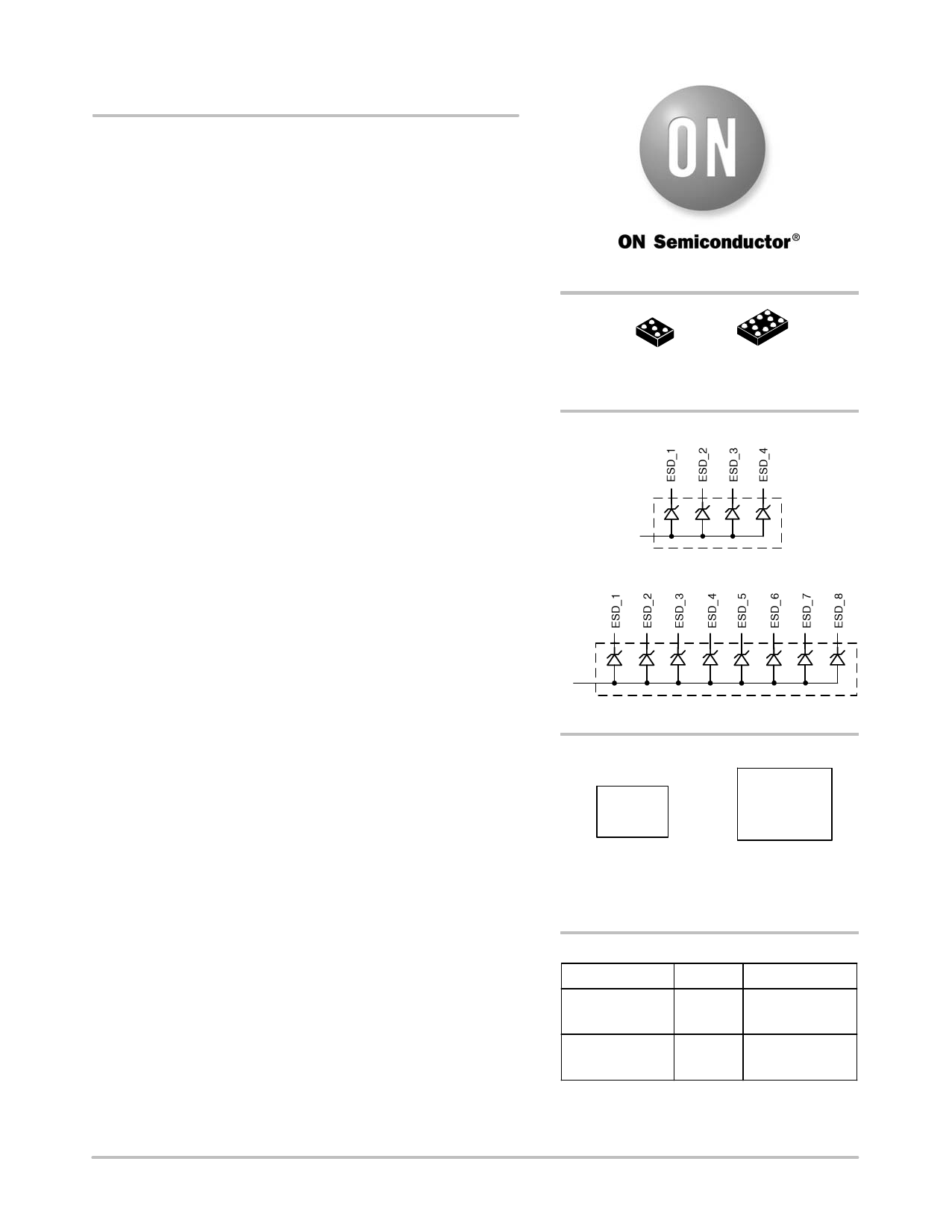
BLOCK DIAGRAM
A1 A3 C1 C3
B2
GND
CM1220−04
A1 A3 A5 A7 C1 C3 C5 C7
B1, B2
GND
CM1220−08
MARKING DIAGRAM
J
L208
CM1220−04
CM1220−08
5−Bump CSP Package 10−Bump CSP Package
J
= CM1220−04CP
L208 = CM1220−08CP
ORDERING INFORMATION
Device
Package
Shipping†
CM1220−04CP
CSP−5 3500/Tape & Reel
(Pb−Free)
CM1220−08CP
CSP−10 3500/Tape & Reel
(Pb−Free)
†For information on tape and reel specifications,
including part orientation and tape sizes, please
refer to our Tape and Reel Packaging Specification
Brochure, BRD8011/D.
© Semiconductor Components Industries, LLC, 2011
1
February, 2011 − Rev. 3
Publication Order Number:
CM1220/D
Share Link: 