APA4880OI-TUL Просмотр технического описания (PDF) - Anpec Electronics
Номер в каталоге
Компоненты Описание
производитель
APA4880OI-TUL Datasheet PDF : 16 Pages
| |||
APA4880
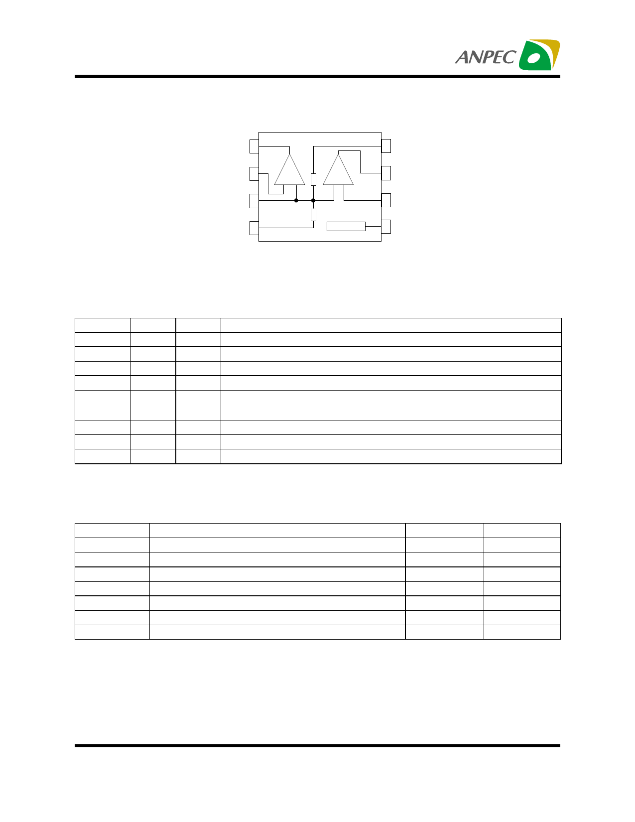
Block Diagram
OutA 1
INA 2
Bypass 3
VSS 4
A
B
-+
+-
MUTE
APA4880
8 VDD
7 OutB
6 INB
5 Mute
Pin Function Description
Pin Name No
OUTA
1
INA
2
Bypass
3
VSS
4
Mute
5
INB
6
OUTB
7
VDD
8
I/O Description
O Channel A output pin
I Audio input channel A
I Connect to voltage divider for internal mid_supply bias
Ground or negative supply voltage connection for circuitry.
I mute mode control signal input, place entire IC in mute mode when held
high, Imute=140µA
I Audio input channel B
O Channel B output pin
Supply voltage input pin
Absolute Maximum Ratings
Symbol Parameter
Rating
Unit
VDD
Supply Voltage
5
V
TSC(O)
Output Short-Circuit Duration , at TA=25°C , PTOT=1W
20
S
TA
Operating Ambient Temperature range
-40 to 85
°C
TJ
Maximum Junction Temperature
150
°C
TSTG
Storage Temperature Range
-65 to+150
°C
TS
Soldering Temperature , 10 seconds
260
°C
VESD
Electrostatic Discharge
-3000 to 3000*1
V
Note : *1. Human body model : C=100pF , R=1500Ω , 3 positive pulses plus 3 negative pulses
Copyright ANPEC Electronics Corp.
2
Rev. A.4 - Jan., 2003
www.anpec.com.tw
Share Link: 