27C1610-10 Просмотр технического описания (PDF) - Macronix International
Номер в каталоге
Компоненты Описание
производитель
27C1610-10 Datasheet PDF : 19 Pages
| |||
MX27C1610
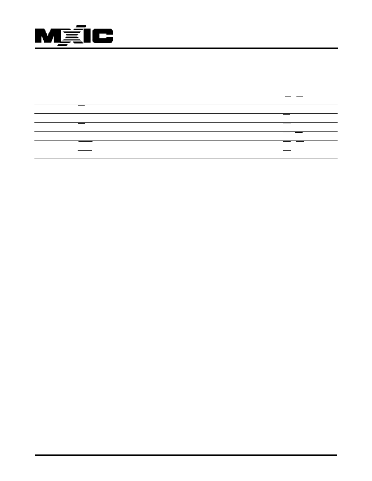
AC CHARACTERISTICS --- READ OPERATIONS
SYMBOL
tACC
tCE
tOE
tDF
tOH
tBACC
tBHZ
27C1610-10
DESCRIPTIONS
MIN. MAX.
Address to Output Delay
100
CE to Output Delay
100
OE to Output Delay
50
OE High to Output in High Z 0
35
Address to Output hold
0
BYTE/VPP to Output Delay
100
BYTE/VPP Low to Output in High Z 50
27C1610-12
MIN. MAX.
120
120
50
0 35
0
120
50
UNIT
ns
ns
ns
ns
ns
ns
ns
CONDITIONS
CE=OE=VIL
OE=VIL
CE=VIL
CE=VIL
CE=OE=VIL
CE= OE=VIL
CE=VIL
NOTE:
1. tDF is defined as the time at which the output achieves the open circuit condition and data is no longer driven.
TEST CONDITIONS:
• Input pulse levels: 0.45V/2.4V
• Input rise and fall times: 10ns
• Output load: 1TTL gate+100pF(Including scope and
jig)
• Reference levels for measuring timing: 0.8V, 2.0V
P/N:PM0593
REV. 1.4, NOV. 19, 2002
10
Share Link: 